
Transparent Devboard
(not so) Transparent Devboard
i unfortunately am currently abandoning the transparent idea, but I've contacted a few manufactures to try and make it happen
Day 1 - Schematic

I'll be basing the dev-board off this module, the ESP-32 C3 Mini. I think the mini form factor is pretty good, while also having alot of great features. I chose to use this module, rather than a custom chip set just in order to increase the reliability of it, but also have it so that the costs were less.
I want to keep this pretty simple, but here are the requirements I set out with.
- Low Profile
- Small Footprint
- Breaks out all GPIO
- More than 1 WS2812B LED
- Power LED
- Programmable Regular LED (Selectable)
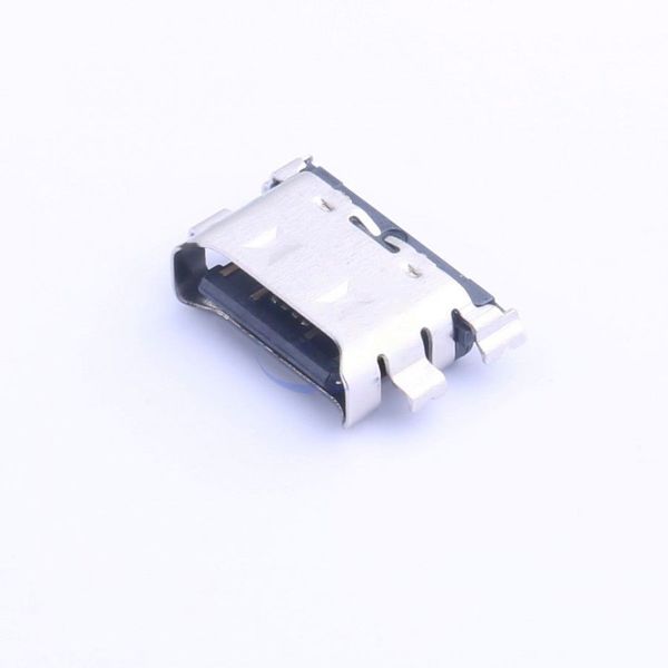
To keep inline with the slim/low-profile criteria, I'll be using this USB port, and honestly, I've wanted to use this part for a while. I think it adds a pretty unique spin on the board.

For the voltage regulator, I didn't really like the bulkiness of the AMS1117-3.3, so I rather went with the AP2112K-3.3. This provides a much smaller form factor, but limits the output current to 600mA compared to 1A.


I then added the standard LEDs, with a jumper on the user one in case it didn't need to be used, the the pin could be used for the GPIO instead.
For the WS2812B led, I went with a much smaller one, helping to fit the criteria of the board. I think these look much better as well, taking up less space.


I then have buttons for both EN and Boot. I chose to use a slightly larger component, but I think these will give a more premium and tactile feedback to the user when using the board.
At the moment, I've just got some placeholder headers in, as I'll end up selecting the final number based on the board size/shape later.
I decided not to do say a battery charging circuit or something similar to be able to cut down on the board size,
Time Spent - 3 Hours (5/07/25)
Day 1.5 - Layout
I've started out with this rough layout of the board, deciding where the key components need to be placed. I didn't really want the PCB antenna hanging off the edge, so I'm going to do a copper exclusion zone underneath, I'll have to see how this goes in terms of effectiveness.

The USB-C port, and both buttons are located at the bottom. The LEDS then sit above those buttons, with their associated capacitors and resistors.

I packed everything in pretty closely, and really like how this looks. Yet, 2 big problems. 1, it'll probably require 4 layers.. meaning making it transparent will be hard. and 2. there is this big open gap in the middle.
To address the first, I'll first be making a regular, rigid version, and then afterwards maybe pursuing a less feature filled transparent one, so ultimately, I want to continue with the board as it is now.
Secondly, there is the big gap of dead space in the middle that kinda harms how the board looks. To fill this, I'll be using a STEMMA QT/ QUICC connector, to allow for easy connection to I2C using the JST SH connector.

This solution turned out very well, and I really like how all the components fit together on the board. The grid-type layout makes it seem very professional, and polished.

The STEMMA-QT port really was able to tie it together, and it now looks pretty cohesive. The board outline is sorta tentative at the moment, but I really like the size as well.
Time Spent - 2 Hours (5/07/25)
Day 3 - Routing

I started off by routing the differential part of USB Data tracks, unfortunately, due to the location of the module and port, and all the components on the surface, these had to go on the back layer, and got a bit cramped with other components.

This is how the top layer turned out. I decided to not use copper pour planes due to the possibility of making it transparent, and then this obviously ruining it.

and I made a kinda big-ish mistake. so my USB-C port is inline with the board, meaning there has to be a cutout. the way the traces are routed currently is umm.. prohibitive of this. the vias would uhh, not exist :)

to fix this, I had to move everything to the otherside of the port. This created some challenges, and I had to move the I2C pull-up resistors in order to accomodate the vias for the data traces. This puzzle to get everything to fit took a while, but was very rewarding in the end.

I'm very happy with how everything turned out looking. It's pretty much just as I had conceptualised, and perfectly meets my criteria.
Tomorrow I'll be working on adding the silkscreen to the back, then getting it ready to ship.
The routing was challenging, but really fun, and it ended up working very well.
I ended up adding an extra hole to the breakout, just to make it fit nice.

I also rounded all the traces, and tomorrow will just be doing some of the final checks, and the back silkscreen for the marking of the pinout.
I'm very pleased with how this is turning out, and the skills that it's giving me.
Time Spent - 5 Hours (6/07/25)
Day 4 - Silkscreen
I did some silkscreen on the back. I kept it pretty simple and professional, labelling all the breakout pints an buttons. Some of it probably should have gone on top, but unfortunately there is alot of space constraint due to everything being so tightly packed.


I'm just now finalising the quotes with the supplier for the transparent PCB, but other than that, I'm ready to submit!!