
Total time spent: 17.5 hours
May 15, 2025
Today, I mostly focused on planning. I want this keyboard to: - Be column staggered - Have more convenient key placements - Feel satisfying to type on - Be overall more intuitive than normal keyboards.
Anaylizing my typing patterns, I notice that my hands often feel cramped, keys feel somewhat unintuitive in location, and I struggle to
hit keys like tab
and backspace
with my pinkie fingers. I decided that it would be best to not have a dedicated function row, and to instead have it accessible with an fn key.
With some thinking, I have made a plan for a keyboard with 52 keys. Currently, I think it'll have only 2 thumb keys per hand, but I might change that later on. For inspiration, I looked on the internet ; especially on the Reddit sub r/ergomechkeyboards.
There, I found some designs that I want to take inspiration from
by u/ianmcl
from u/pedrorq
the ZSA Voyager.
With a good idea of what I wanted to make in mind, I have started to plan out the layout for my keyboard.
Time Spent: 2.5 hours
May 16, 2025
Today, I started designing the left half of my keyboard.
However, before that, I finished tweaking my keybaord design on Keyboard-Layout-Editor
This is what I came up with. I've decided to increase the amount of thumb keys to 6, so this will be a
54 key keyboard.
I also decided that I want to use low profile switches. I've tried to use normal profile keyboards in the past, but the height makes my wrists hurt.
The thing is, unlike regular profile switches, there isn't really a standard design for low profile switches. I had to go hunting for footprints, 3d models, hotswap sockets, etc for the Gateron KS-33 switches I chose to use.
One I had my layout finalized, it was time to star schematic-y-ing. That was fortunately pretty straightforward.
It was when I loaded up the pcb that I came across a problem. How was I going to properly postition all the keys? Now this
isn't my first rodeo with keyboard-related designs, but this is the first one I've had one with a column stagger and angled switches.
To make accomplish this task, I headed over to ai03 where I generated plate for my design. At first, the edges of the
cutout were rounded by default, but I removed this for convenience. I then downloaded it as a dxf and imported it into Kicad as a graphic.
I also edited the Gateron KS-33 footprints I had found to so that they would have a centered 14x14 box in them, the same dimensions as the switch plate. This allowed my to postion the switches relatively to the plate.
Next, I need to place the diodes and add edge cuts!
Time Spent: 3 hours
## May 17, 2025 Today I finished my PCBs, and started making the cases. It was sooooo tedious trying to place everything where it needed to be, finding footprints, 3d models, editing footprints, etc. Closer to the end of the process, I decided it would be best to change the keyswitch footprint from this one by siderkb on Github
I was not tryna do allat, so after completing the left half of my keyboard, I simply made copy of it, renamed it, and flipped the copied pcb in kicad.
I then proceeded to flip certain elements, reroute, and update the schematic a bit for a proper design.
Here's what it looks like looks like:
A bit of a tangent, but you may have noticed a blocky grey thing near the thumb keys on my pcb. This is what will allow the two keyboard halves to communicate with each other! Normally, split keyboards use a TRRS jack to facilitate this communication. They look like this! The thing is, TRRS is not hotswappable. This means that if you accidentally unplug the connector cable while the keyboards are connected to power, very bad things will happen. I'm kinda clumsy, so that option was out.
Less commonly, USB-C is also used, but I decided to avoid that because it's hard to solder and I didn't want to use it non-standardly.
I decided to used a RJ11/6P4C connector because it is hotswappable and pretty easy to solder. It is a bit chonky, but that just means it has personality :)
With my pcbs done, it was time to start on the cases. To make my job a lot easier, I exported the edgecuts layers and a couple other as SVG's. I then converted the SVG file to DXF, and imported it into a new Fusion360 project. This allows me to design my case very accurately to my pcb
At the moment, I am currently struggling to offset my case outline properly, because apparently the universe finds spiting me funny TT. As you can see,
a few segments of the outline are not included for some reason
Maybe it'll work tomorrow...
Time Spent: 5 hours TT
May 19, 2025
I figured out how to offset my case outline! It turns out that if you zoomed in really really close, the lines weren't properly connected. I fixed this, and everthing went swimmingly.
Until....I looked at the Gateron KS-33 data sheet. To my surprise, the max distance that can be between the pcb and switch is 2.5 millimeters.
Now, with regular, non-low-profile switches, the maximum distance that can be between the pcb and switch is 5mm. I plan on getting my my switch plate 3d-printed. It's reccomended that a 3d-printed switch plate be at least 3mm thick, to prevent bending. For a brief but not insignificant moment, I considered using normal profile switches. But, I decided I really didn't want a tall keyboard. I will thug it out.
With that decision made, I finished designing the right half of my case pretty quickly. With a strong idea of what my casing will look like, the left half
shouldn't take too long(I jinxed it, didn't I?).
I also got the boilerplate for my firmware done! I just need to figure what keys I want to put on each layer, and I'll be done
Bonus: When importing a 3d model of my PCB into Fusion360, I noticed that I had accidentally put a diode on the front-side instead of the back side. Oops. Stay observant y'all!
Time Spent: 4 hours
May 20, 2025
I finished! Fortunately, I did not in fact jinx it. My cases are looking very handsome in the README, if I do say so myself.
While examining the CAD for my left case, I noticed that I had accidentally flipped the RJ11 jack the wrong way on my PCB. Fortunately, it
was an easy fix.
Since there is going to be a spot where the pcb is visible, I added some silkscreen branding and a little bit of art. I'm quite pleased with how it looks.
Finally, I made my firmware! It wasn't hard, but it did require switching between a lot of different tabs. I also had to learn how layers work in KMK, which was interesting.
Time Spent: 3 hours
June 19, 2025
Today I attempted to assemble my keyboard. Emphasis on the word attempted
everything was actually going swimmingly, with no major hiccups. Soldering was tedious, but not hard.
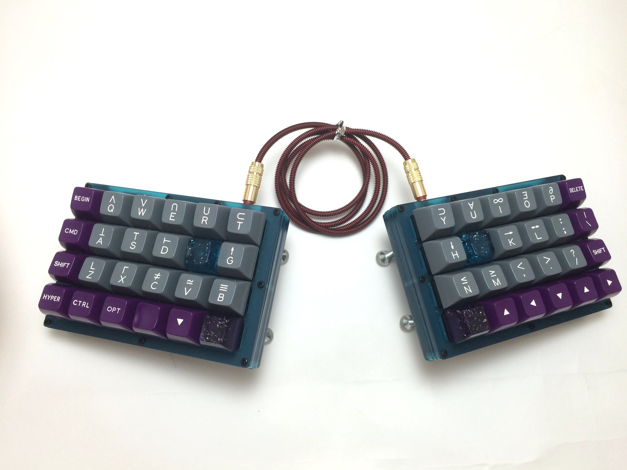
When I was done, this is what it looked like
To check that everything was working, I went into the Thonny editor, and bridged each of the hotswap sockets. Save one that I had forgotten to finish soldering, everything was working.
The problems started when I tried to connect the two halves. Long story short, it turns out I had made a mistake in the pcbs, accidentally connect gnd to power and power to gnd.
Luckily, it was a fixable mistake, and I destroyed the existing traces in favor of some copper wire I had. I accidentally destroyed one too many traces though, so I had to solder an extra wire.
When I connected the two halves, I noticed that both microcontroller would only light up when plugged into the right side. Another long story short, the microcontroller went on strike and refused to let me upload firmware on it.
I also got the 3d printed case in the mail today( thanks Logan!). The corner of the right half was a little bit warped, so I had to do some sanding. But, when I put the switches in the right half, the scab(traitor) I realized that the keys furthest from the screws would only register key presses if I pressed down really hard. For some reason, the hotswap sockets were not holding them tight enough.
So, that was a complete failure! But, hope is not lost(yet). I've ordered some more diodes and a (hopefully) functioning microcontroller. I plan on retrying on my extra pcbs, but without the hotswap sockets. Let's hope it works.
Time spent: 6 hours
June 25, 2025
Good news! The right half works perfectly with QMK! The bad news?
The left hand microcontroller is busted.
It all started when I had finished soldering the switches. I went to test everything. Some switches didn't register, so I went back to make sure they were soldered properly. This seemed to fix the problem of all such switches except one. The a
key. That specific failure felt targeted(my initials are both a
).
After a bunch of testing, I determined that the problem was not a mistake in the pcb, diode mis-orientation, or soldering. Even if I shorted the pins directly on the mcu, it still wouldn't work. After some asking around, I've discovered that the controller was probably busted from an accidental static shock. -sigh-
I've decided that it is not a good idea to expose my left hand microntroller, so I've printed a new plate for it. Since I had soldered the switches to the original plate, I had the desolder them. I used a bunch of flux, and to my great surprise, desoldering was really easy! I used braid, which is not known for efficiency, but the fact that the switch holes were so big and filled with so much solder was really helpful. I had everything done in like, 15 minutes.
I'm going to handwire the left half, and hide the mcu under the case. Since the usb port will be inaccessible, I'll make the right half the master half.
The new plate. It has holes for the rj11 jack to go into.
June 27, 2025
Ngl, building this keyboard has been quite the sucky experience. Five microcontrollers and four of them have all just... died. FOUR! To be fair, one was my fault, damaged from attempting to remove it, but three others is just too much. On the one hand(quite literally), the right hand of my keyboard works perfectly! On the other, the left half refuses to work. I swear, that side must be bad luck or something because all 4 microcontrollers have been broken in an attempt to get that side working. At this point, I might just have to turn the Prince54 into the Prince54.
I've ordered one more microcontroller(with my money, not Hack Club's). Five's the charm?
July 6, 2025
As of Jyl 6, 2025, this keyboard is fully functional! Everything works.
Time Spent: 8 hours