
Hackpad
A custom macropad with rotary encoders, a screen, and a lotta keys
Journal
[!NOTE]
Total time spent: 60h
27/06/2025
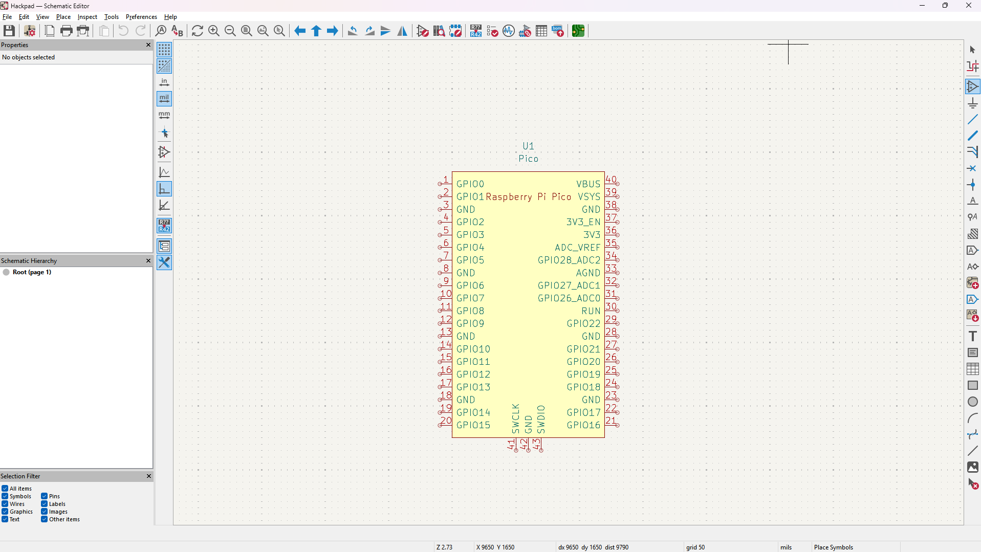
I did some research on different microcontrollers I could use. I first landed on the Elite C, but every single site I looked on was out of stock ;-;, so maybe not a good choice. Eventually I decided on the Raspberry Pi Pico compared to the XIAO RP2040 in the Hackpad tutorial, because its got a lotta more GPIO, and even though its bigger for me thats fine (I think, so far). I might integrate a Micro USB to USB C adapter though, I REALLY want USB C lol.
Found this Github Repo with the 3D footprint etc of the Raspberry Pi Pico for KiCad. Installed it and set it up.
[!NOTE]
Total time spent: 1h
28/06/2025
Going to use the SSD1306 128x64 screen:
- Purchase Link: https://thepihut.com/products/0-96-oled-display-module-128x64
- KiCad Symbol: https://github.com/pforrmi/KiCad-SSD1306-128x64 (Not in the official KiCad Symbol Library)
- KiCad Footprint: https://kicad.github.io/footprints/Display
- KiCad 3D Model: https://kicad.github.io/packages3d/Display
Ok so after discovering https://github.com/joe-scotto/scottokeebs/tree/main/Extras/ScottoKicad I've just switched to using that because it has symbols, footprints, and 3D models of a bunch of different OLEDs and switches which is nice. This OLED is cheaper and fits the footprint / 3D model: https://thepihut.com/products/0-96-oled-display-module-128x64.
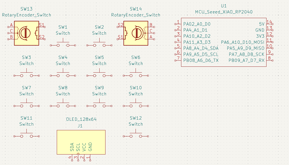
- Rotary Encoder: https://mechboards.co.uk/products/rotary-encoder?variant=40330076651725
- Keycaps: https://mechboards.co.uk/products/ddc-choc-pbt-blank-keycaps?variant=47587896426701 and https://mechboards.co.uk/products/ddc-choc-pbt-blank-keycaps?variant=47405364576461
- Switches: https://mechboards.co.uk/products/lowprokb-ambients-silent-linear-nocturnal-choc-v1?variant=47588169908429
Back to seed XIAO because now doing 10 keys instead of 20.
Really useful video on a key matrix that helped me visualise it: https://www.youtube.com/watch?v=7LyziNdFlew. Back to Raspberry Pi Pico because the Seed XIAO RP 2040 STILL needs 1 more GPIO for me to use it ;-;.
[!NOTE]
Total time spent: 3h
29/06/2025
Finalised parts after a lot of searching (nice!nano v2 for Bluetooth communication):
Mechboards
- 2x 10 lowprokb Choc (V1) Ambients Nocturnal.
- 1x 10 DDC Choc (v1) PBT Blank Keycaps (White Keycaps / 1u).
- 1x 10 DDC Choc (v1) PBT Blank Keycaps (Black Keycaps / 1u).
- 2x 10 Choc V1 Hotwsap Sockets.
- 1x 50 Throughole Diodes.
- 1x nice! nano v2.
PiHut
- 1x 1200mAh 3.7V LiPo Battery. [CHANGED LATER TO WAY SMALLER ONE].
- 1x Adafruit Micro-Lipo Charger for LiPoly Batt with USB Type C Jack. [REALISED LATER I DON'T NEED]
- 1x Breadboard-friendly SPDT Slide Switch.
- 1x 20 Tactile Button switch (6mm).
- 2x Rotary Encoder + Extras.
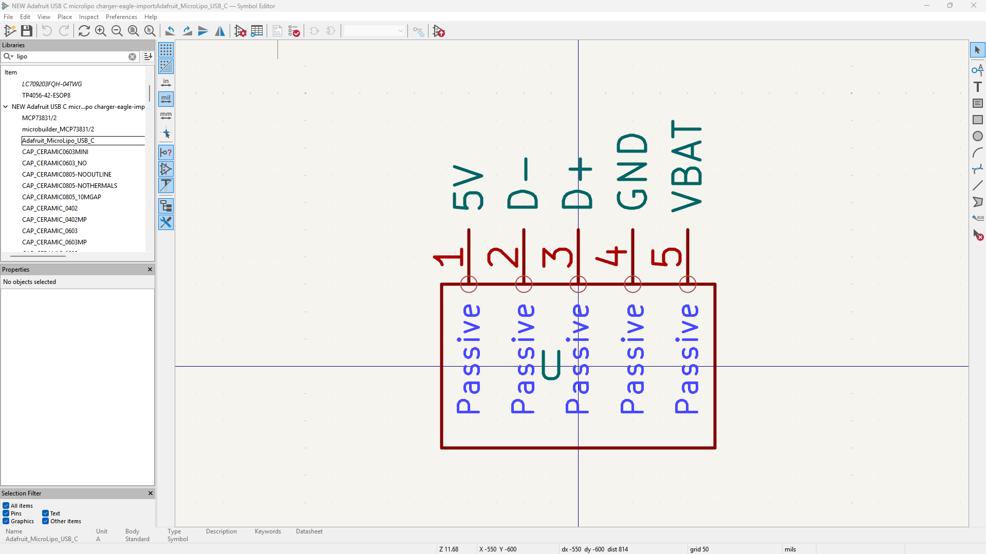
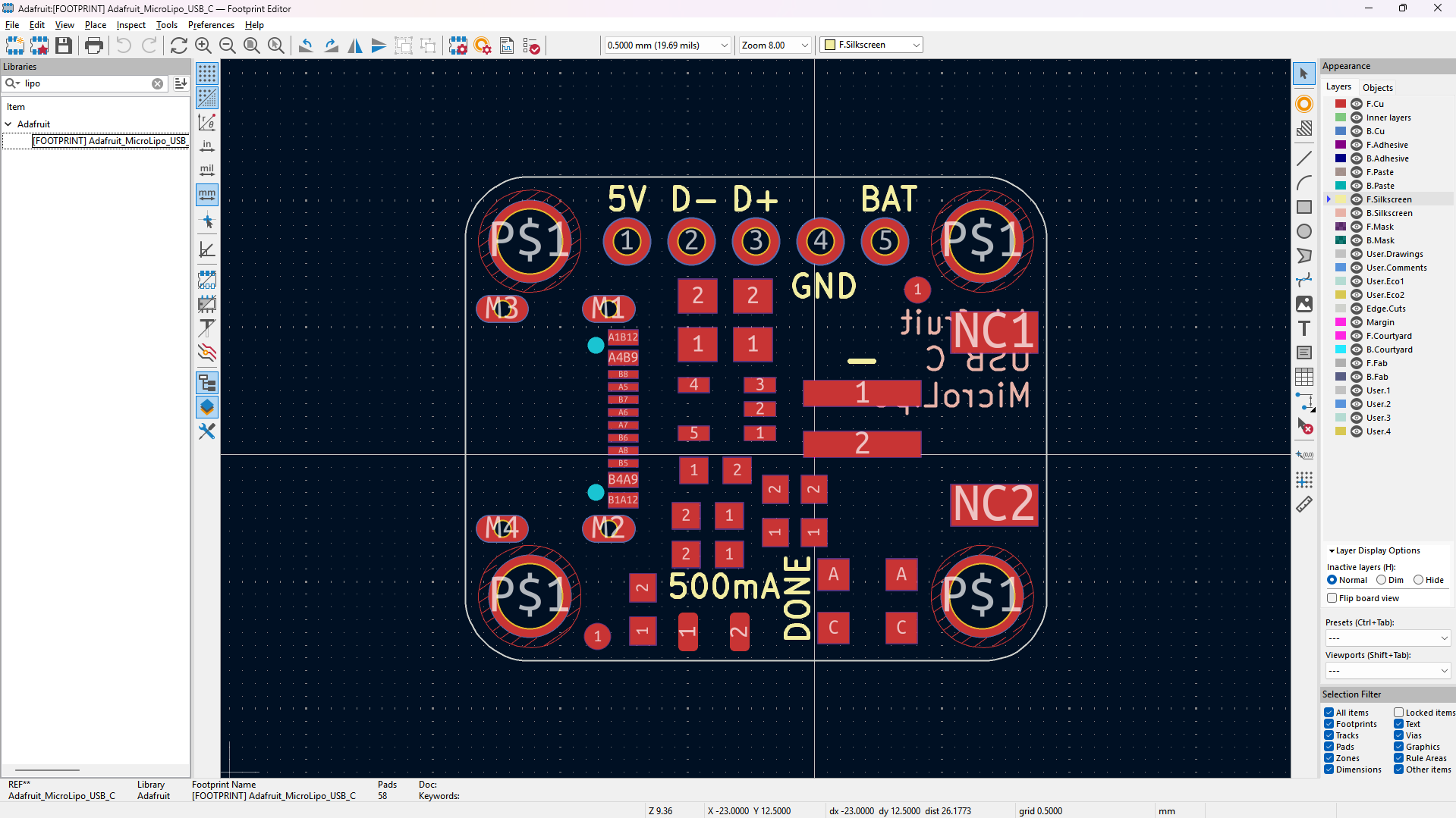
Found the PCB files for the Adafruit Micro-Lipo charger but they weren' for KiCad (.brd / .sch) file type. After converting it (which took a LOT of time ;-;) I realised they were actual PCB files for the board, so I had to create my own schematic of how I would interface with it, not the board itself.
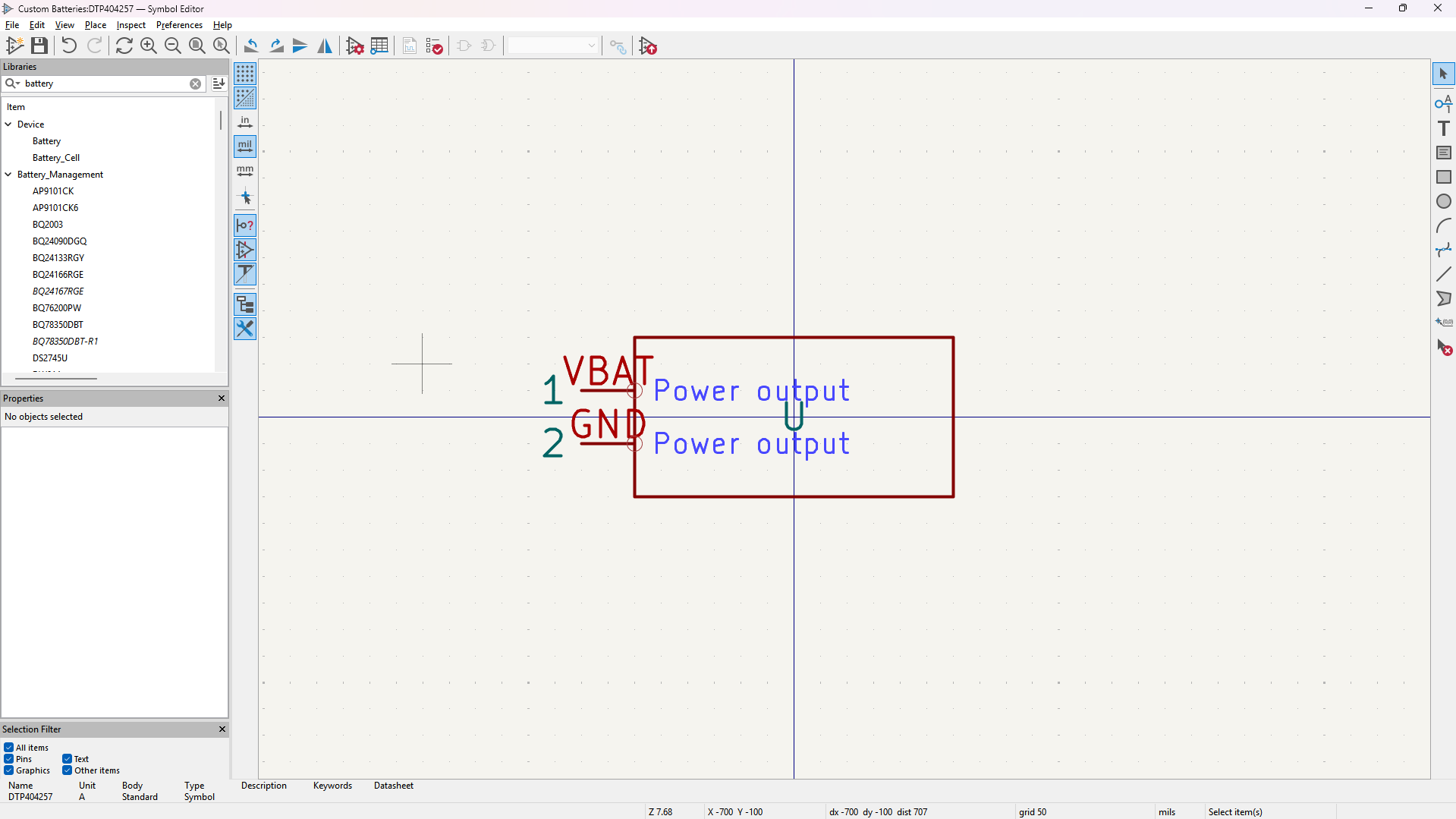
Custom symbol based on the schematic of the board:
Some silkscreen stuff got messed up but I still managed to get the general dimensions of the PCB into a footprint:
Schematic by the end of the day - I switched a bunch of the symbols to specific ones for my parts, etc:
[!NOTE]
Total time spent: 6h
30/06/2025
Created a custom symbol for the 1200mAh 3.7V LiPo Battery.
Nevermind I found the KiCad symbol and footprint for the connectors used in the battery - https://www.snapeda.com/parts/PHR-2/JST/view-part/, so I'm going to use the symbol from there.
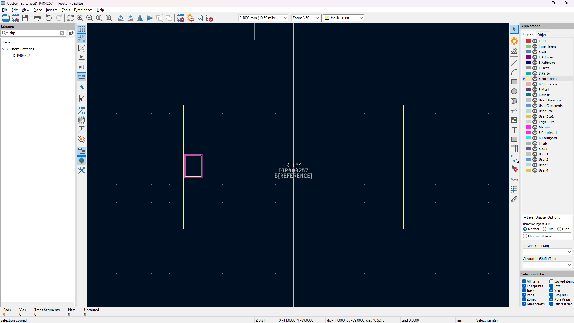
Made a simple footprint for the Battery, without pins as those plug into the Adafruit Micro-Lipo Charger.
I've now realised the Battery stuff has no use because I should interface with the LiPo charger instead...
Found the 3D model of the switch from PiHut, but it doesn't have a symbol or footprint (time to make it :sob:). About 20 minutes later - nevermind I found the symbol and footprint on JLCPCB, and through the linked EasyEDA stuff I exported it and imported and linked 'em in KiCad!
How do you charge the nice!nano?# The nice!nano has a Li-Po charger built in that uses the USB-C port to charge the Li-Po at a rate of 100mA.
Oh great. WHY DID I MISS THIS :sob:. I don't need the Adafruit charger now ;-;.
How to do a switch with the JST thingy: * https://www.youtube.com/watch?v=K1CbrNh6a1s * https://learn.adafruit.com/on-slash-off-switches/overview
The battery will connect with the JST PH 2-Pin Cable - Male Header, this makes it longer, and this will be unpluggable and used for all batteries. This then will be cut and soldered with the switch (so I will buy the JST-PH 2-pin Jumper Cable - 100mm long for extra wire in case I make some mistakes, and also Heat Shrink Pack to insulate around the soldered joints). Then the black end goes to GND (SAME AS OTHERS), red to BAT+ which is BATTERY (top right).
Schematic by the end of the day:
[!NOTE]
Total time spent: 5h
01/07/2025
Swtiched to this battery https://thepihut.com/products/150mah-3-7v-lipo-battery - other one is overkill and this is smaller lol.
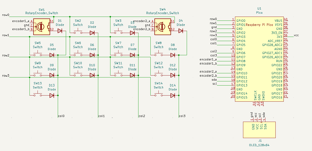
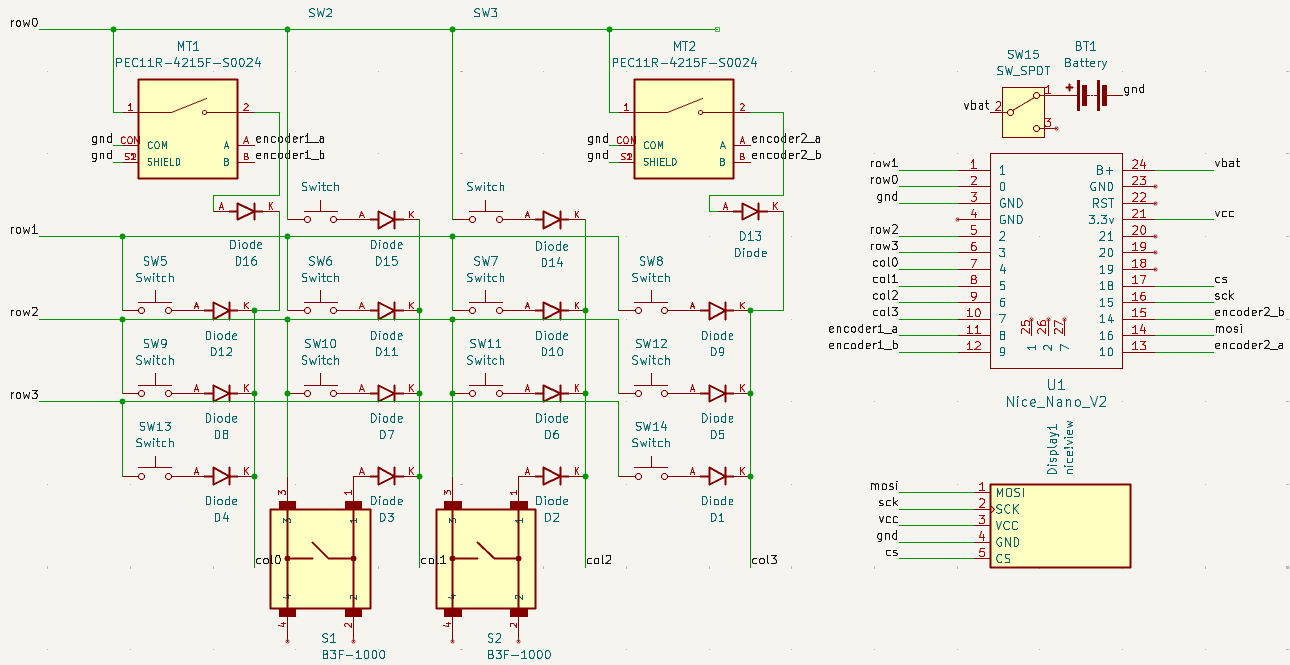
I now realised theres a difference between high and low frequency pins, so after a bit of general schematic cleanup and reordering of GPIOs, I finished with this (now the whole key matrix is on low freq so there isn't a mix of high / low freq GPIO):
Great helping source / documentation: https://docs.splitkb.com/product-guides/aurora-series/build-guide/diodes.
[!NOTE]
Total time spent: 4h
02/07/2025
Sorry for like no journalling today lol but I did a LOT on the PCB design (except for routing) for now (will probably change the bottom buttons later).
Slight problem here:
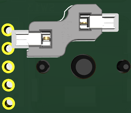
Fixed here:
Switches were upside down ;-;. So the above was useless... (as when the RIGHT way up they did NOT collide).
So I fixed that.
[!NOTE]
Total time spent: 5h
03/07/2025
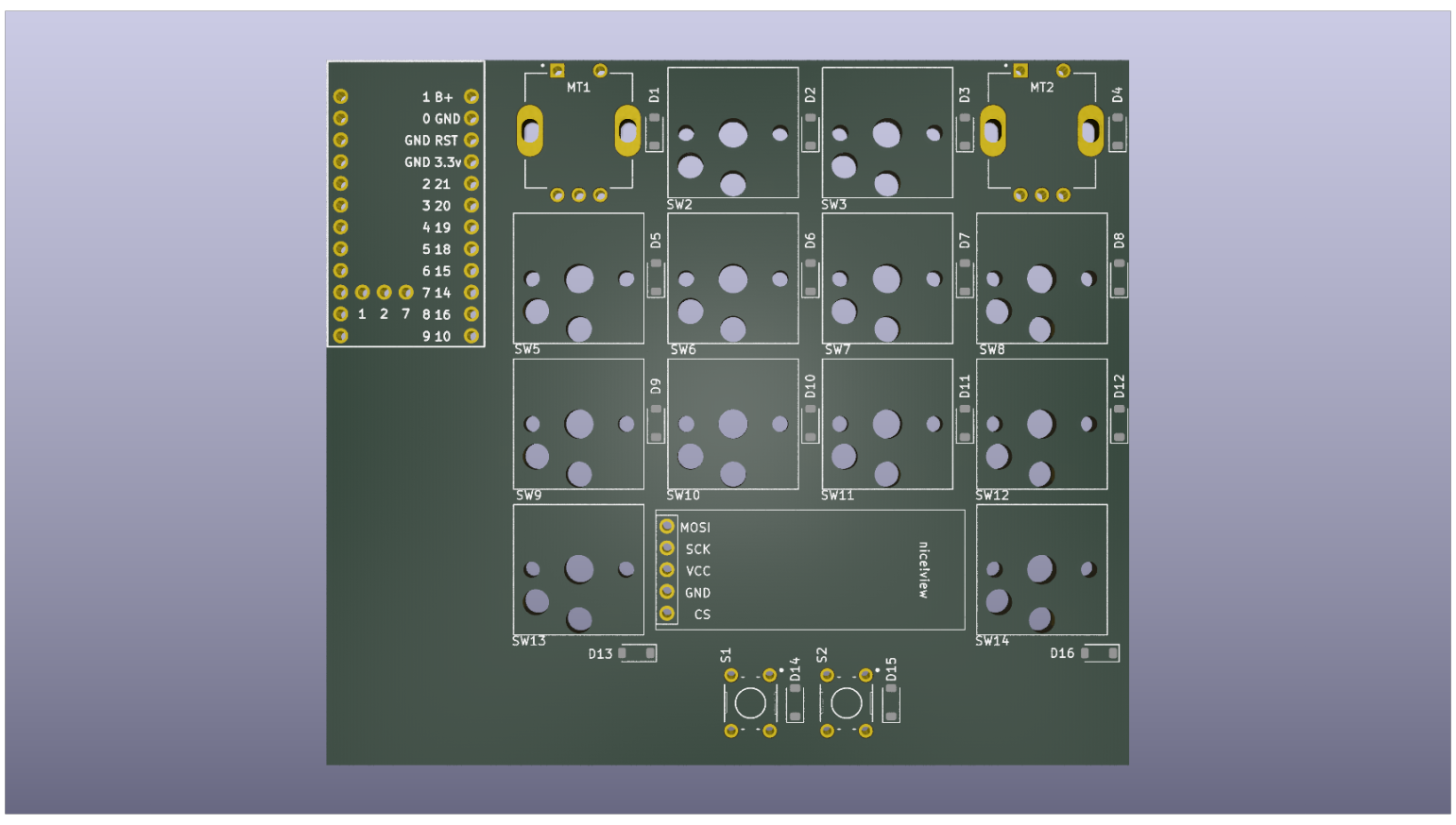
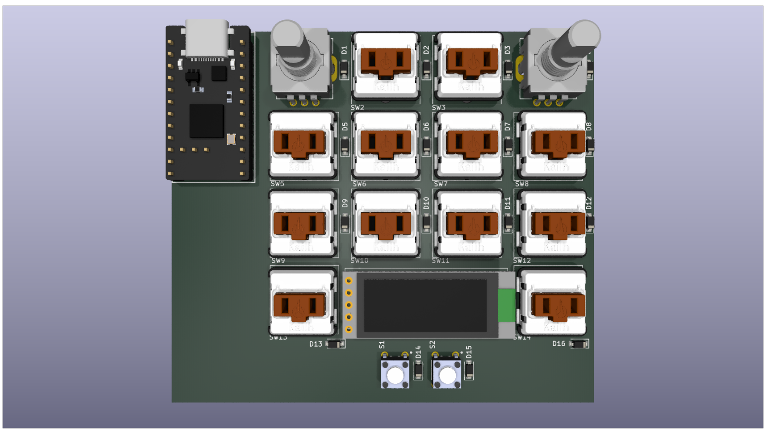
Spent most of today getting some more 3D models into KiCad and reordering some stuff like diodes etc:
[!NOTE]
Total time spent: 2h
04/07/2025
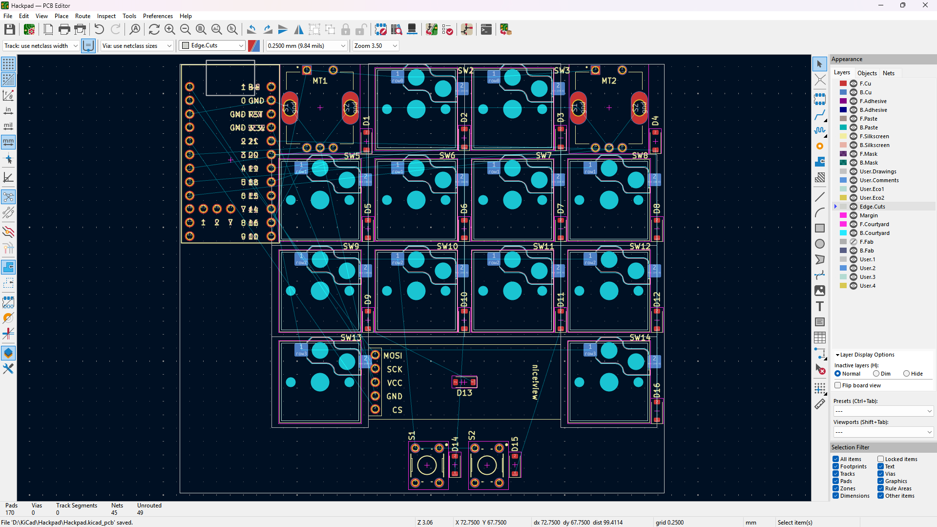
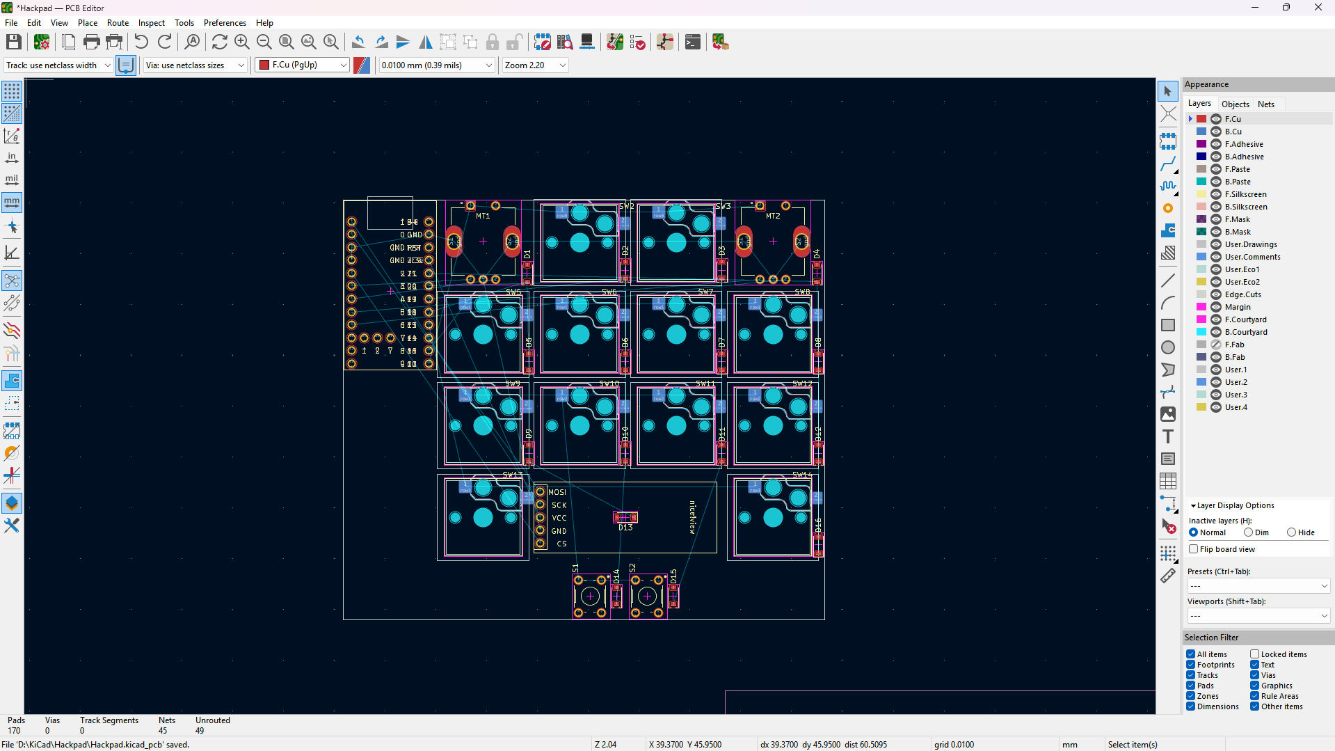
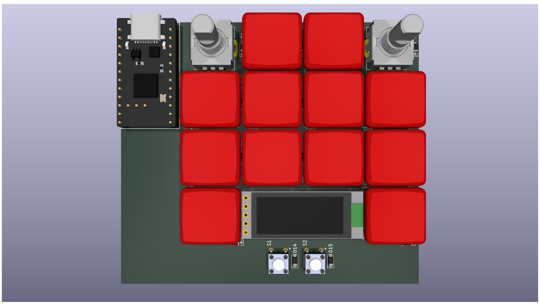
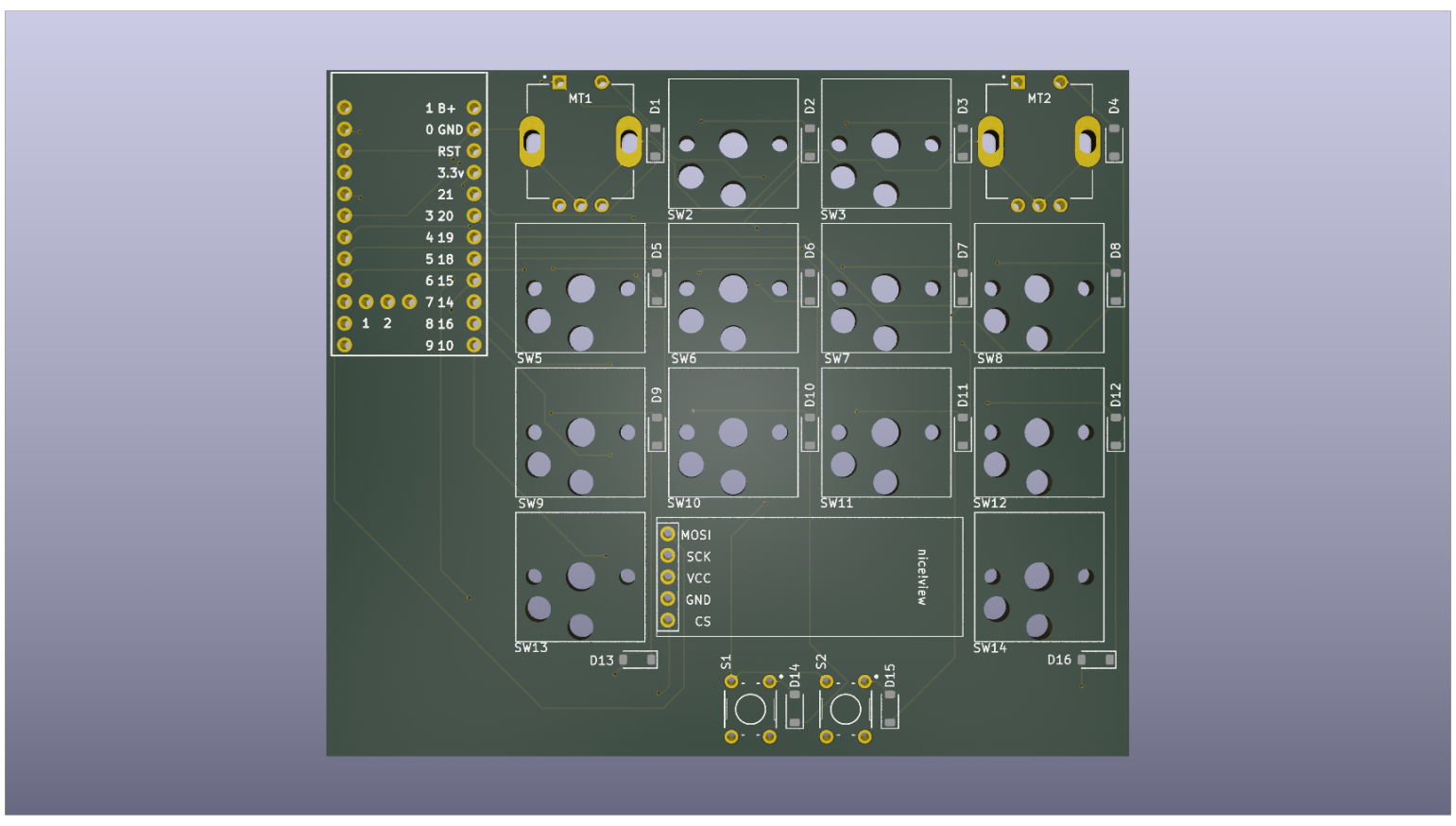
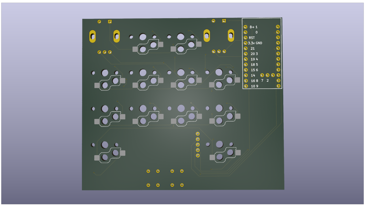
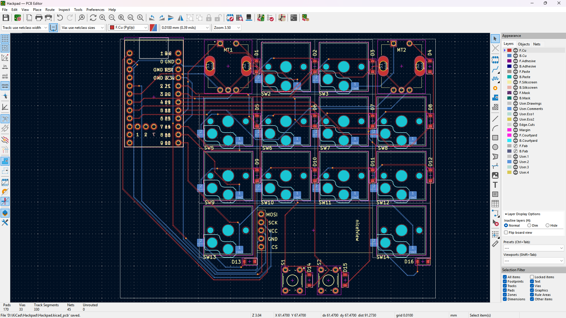
Finished PCB layout, now just need to route it.
Changed the right of the schematic for the nice! nano v2 to this which makes more sense (lower rows lower down so the wiring is cleaner):
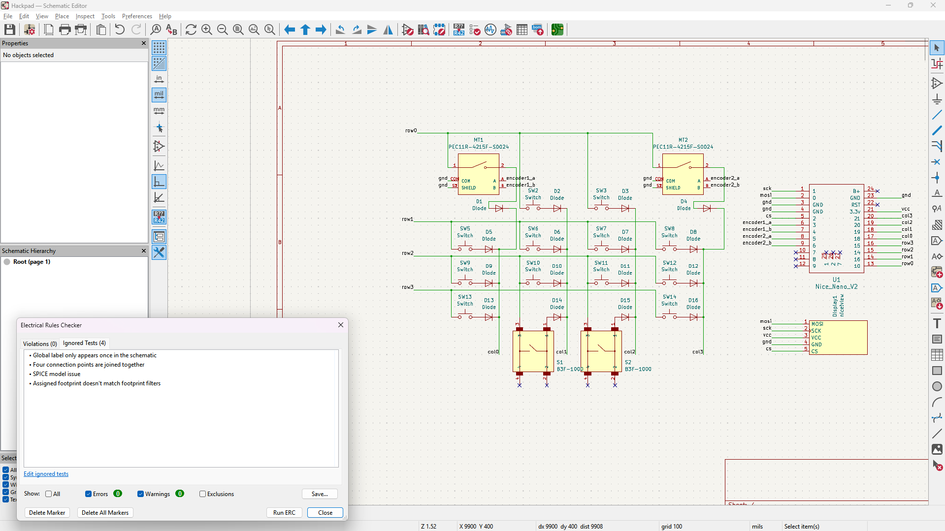
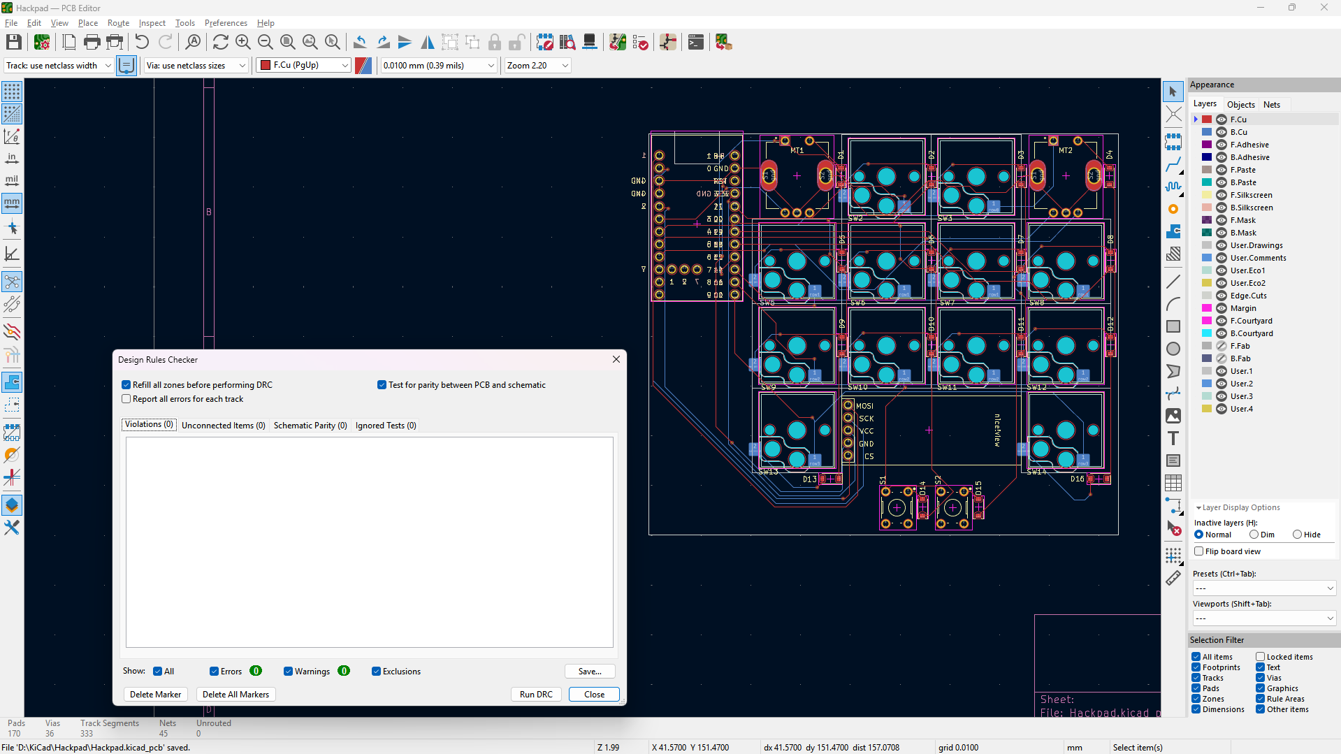
FINALLY finished the wiring (no warnings or errors in DRC).
[!NOTE]
Total time spent: 5h
05/07/2025
Imported the PCB into Autodesk Fusion 360 and started to design the case (ignore the workspace name, I use Fusion for another competition called F1 in Schools lol)
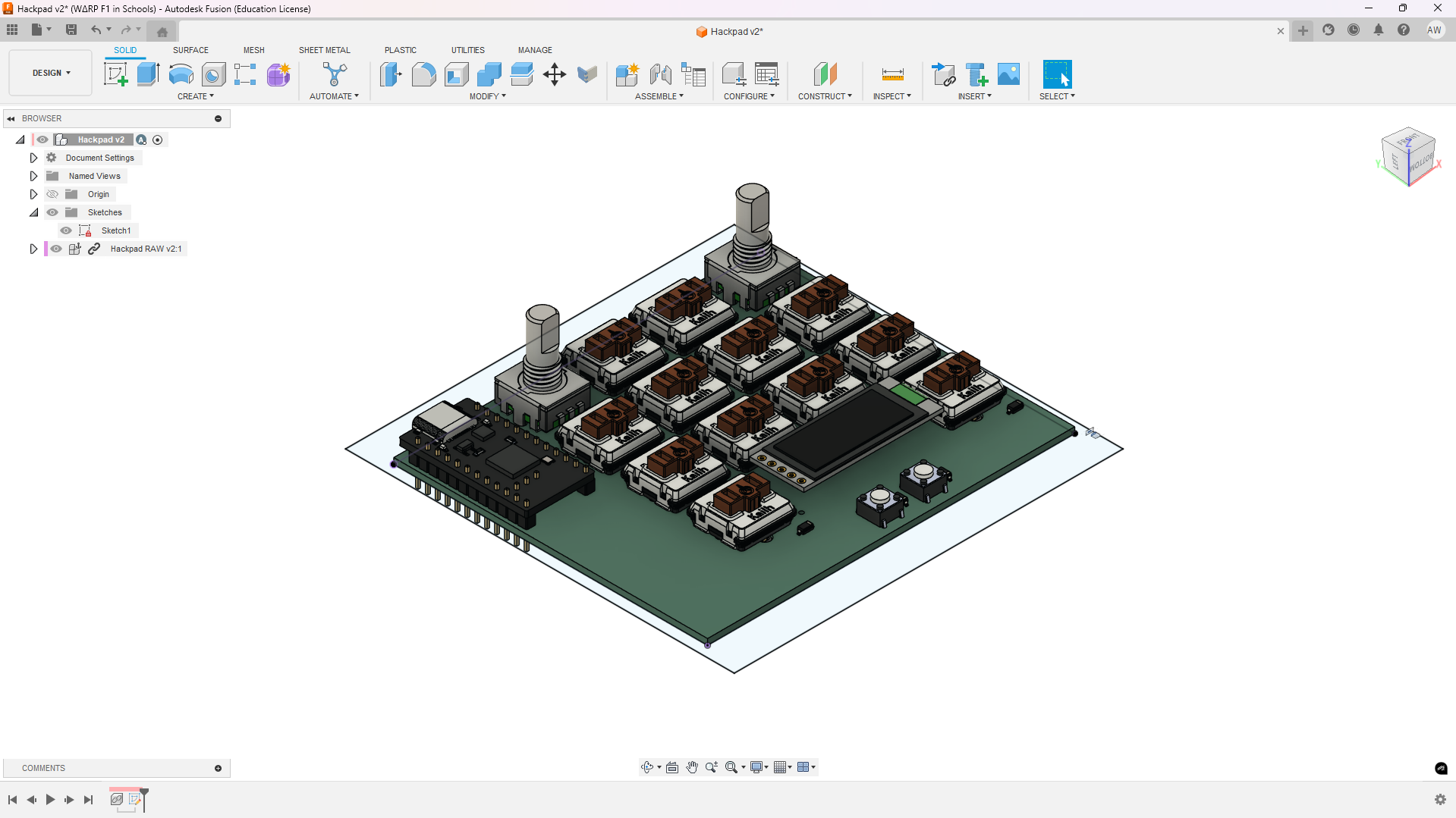
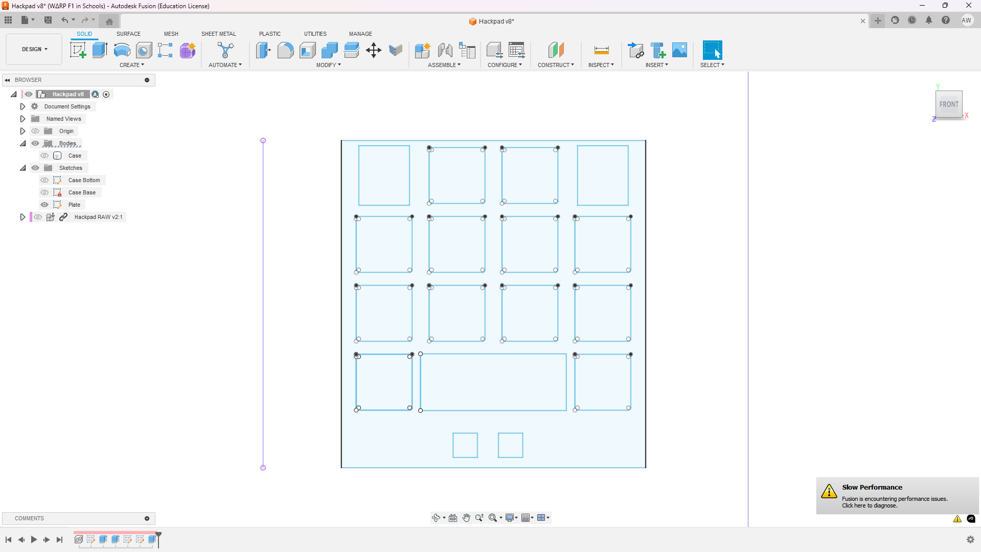
Made a simple square base of the case:
[!NOTE]
Total time spent: 1h
06/07/2025
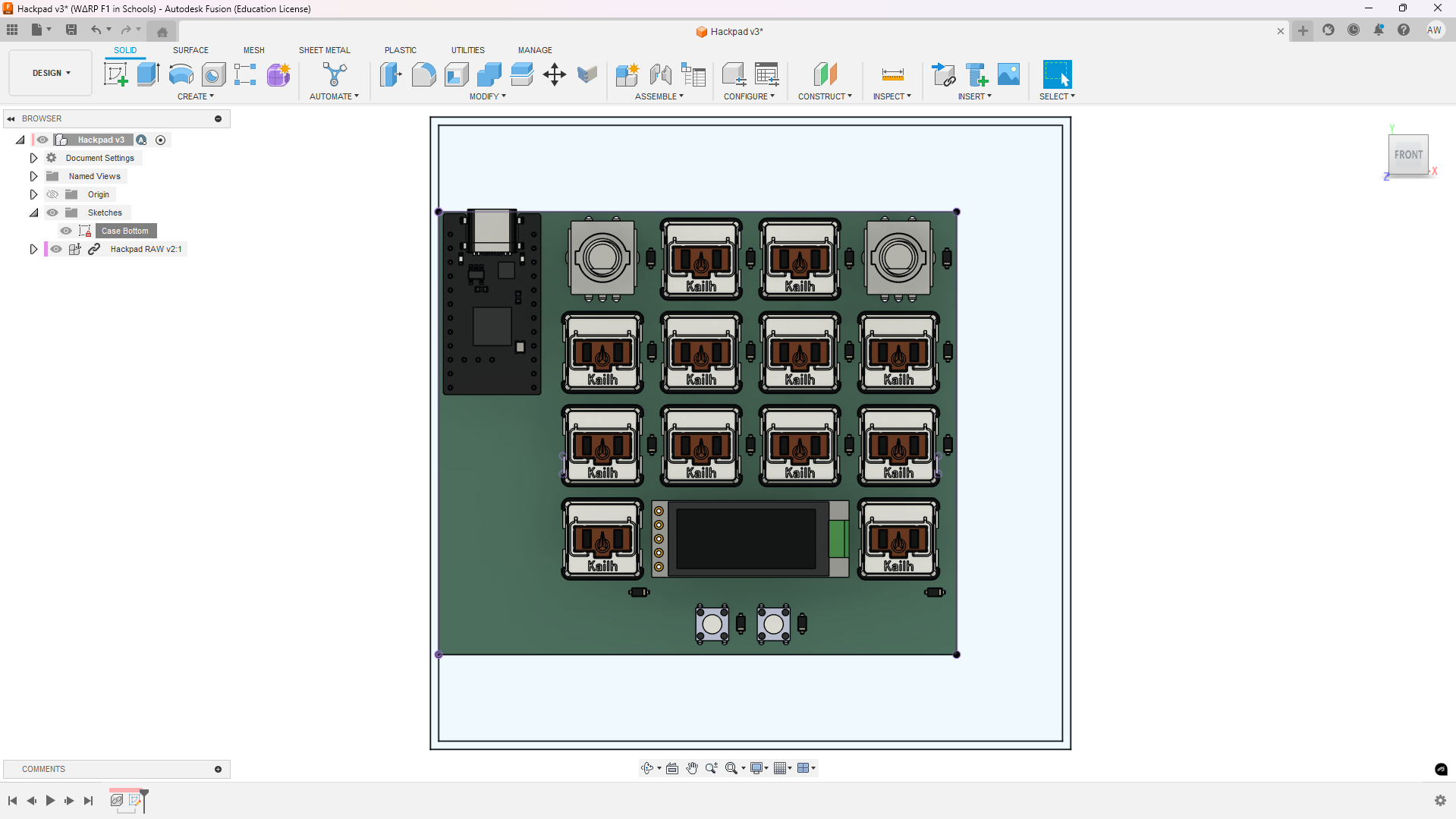
Fixed some of the parameterisation of the case:
Finish plate sketch (dw about the bottom right warning, I'm updating my drivers rn LOL):
[!NOTE]
Total time spent: 2h
08/07/2025
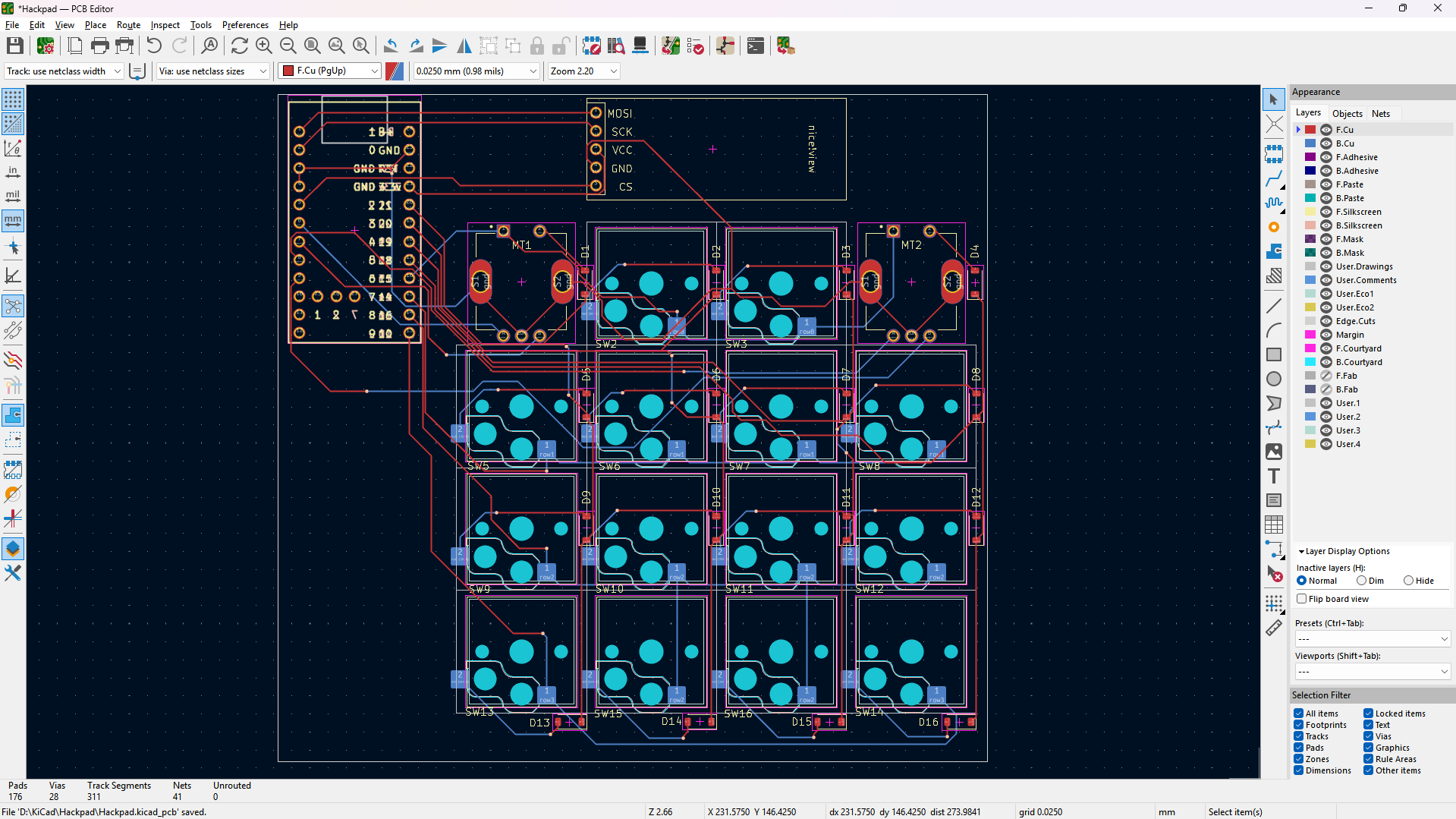
Moved the microcontroller a bit to the left on the PCB to add more space (had to redo wiring, save me pls).
[!NOTE]
Total time spent: 1h
09/07/2025
Redid design AGAIN lol ;-;.
[!NOTE]
Total time spent: 1h
17/07/2025
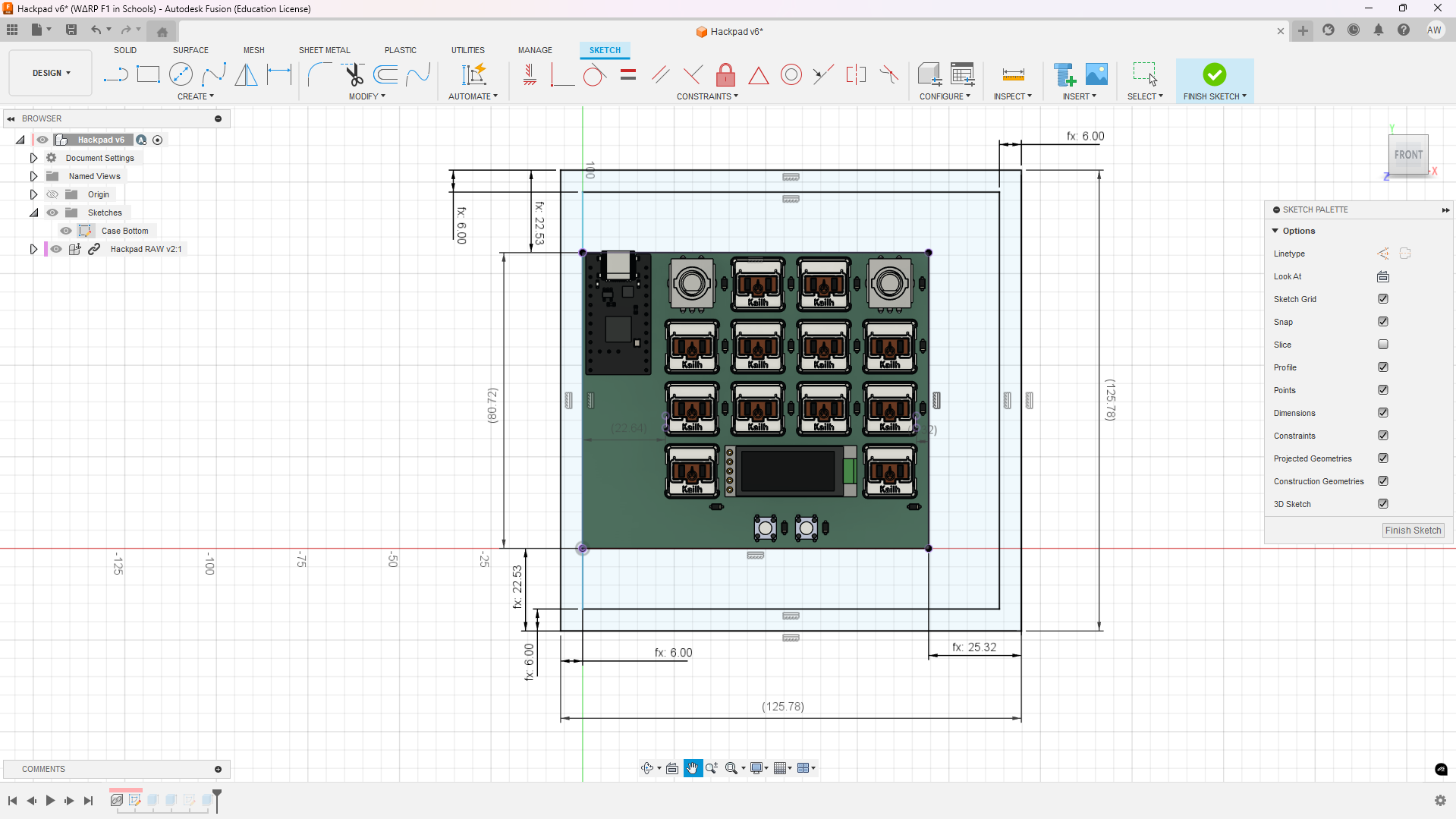
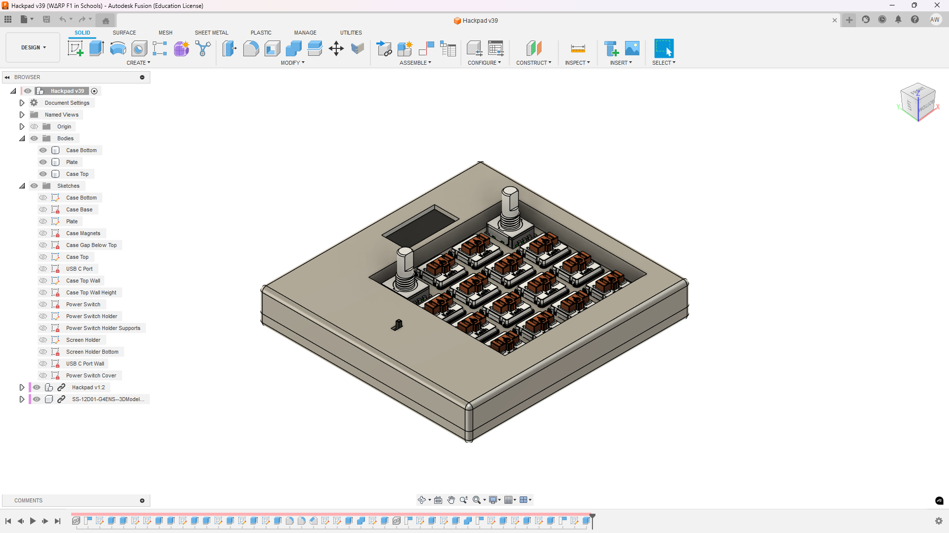
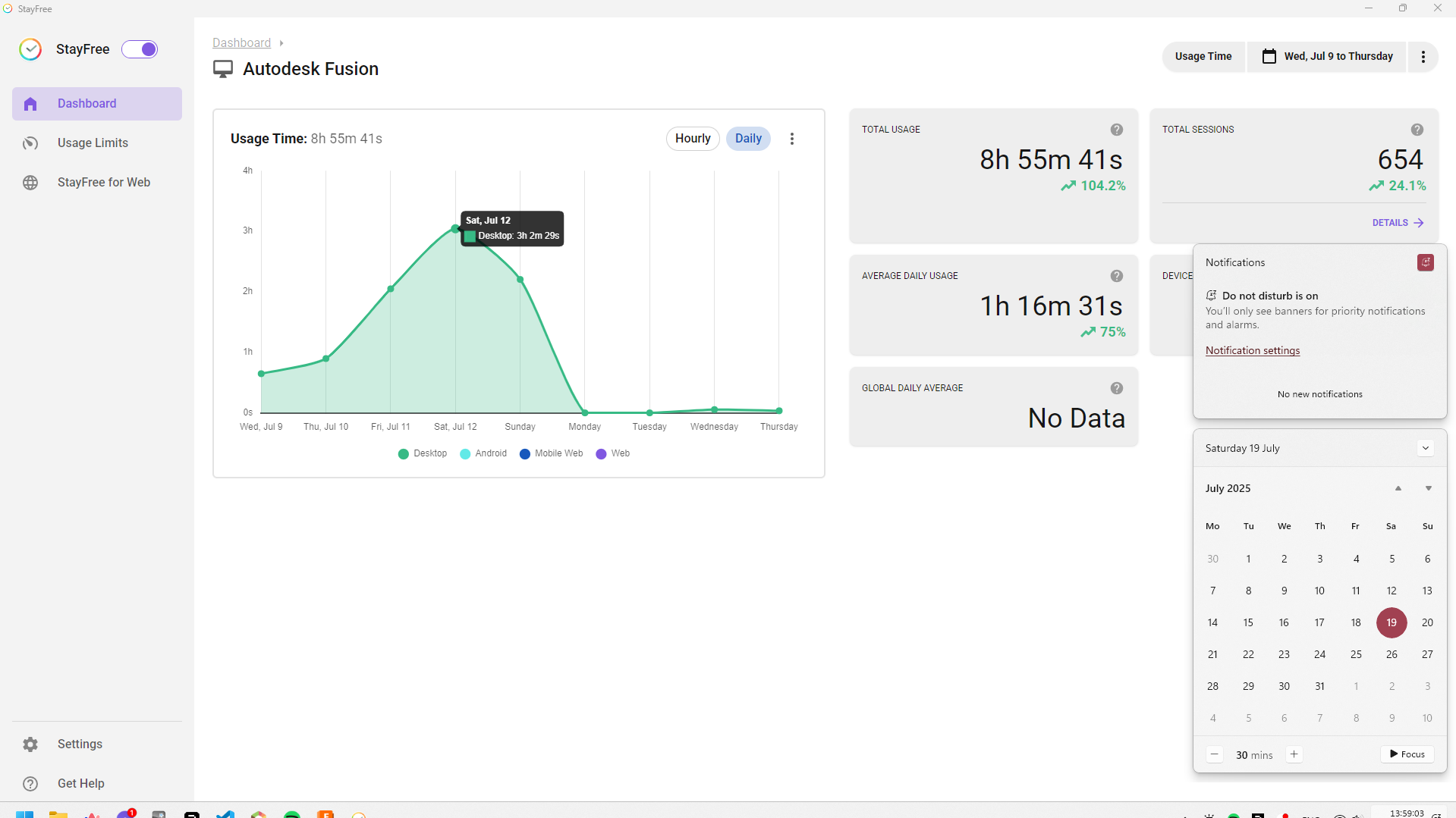
I had some work stuff from the 14th - 16th, but the case is finally finished! I'm really sorry for not journalling most of this but it was so tedious and annoying that journalling was just in the back of my mind the whole time. You can see from the amount of sketches and how the version number has incremented the amount of work it has taken ;-; (I have attached proof below though from my time tracker software).
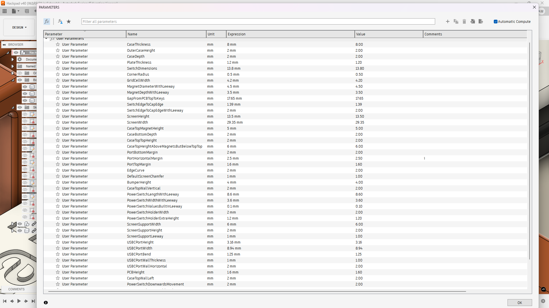
The parameters tab 😭 (its all for a good cause - flexibility):
[!NOTE]
Total time spent: 9h
20/07/2025
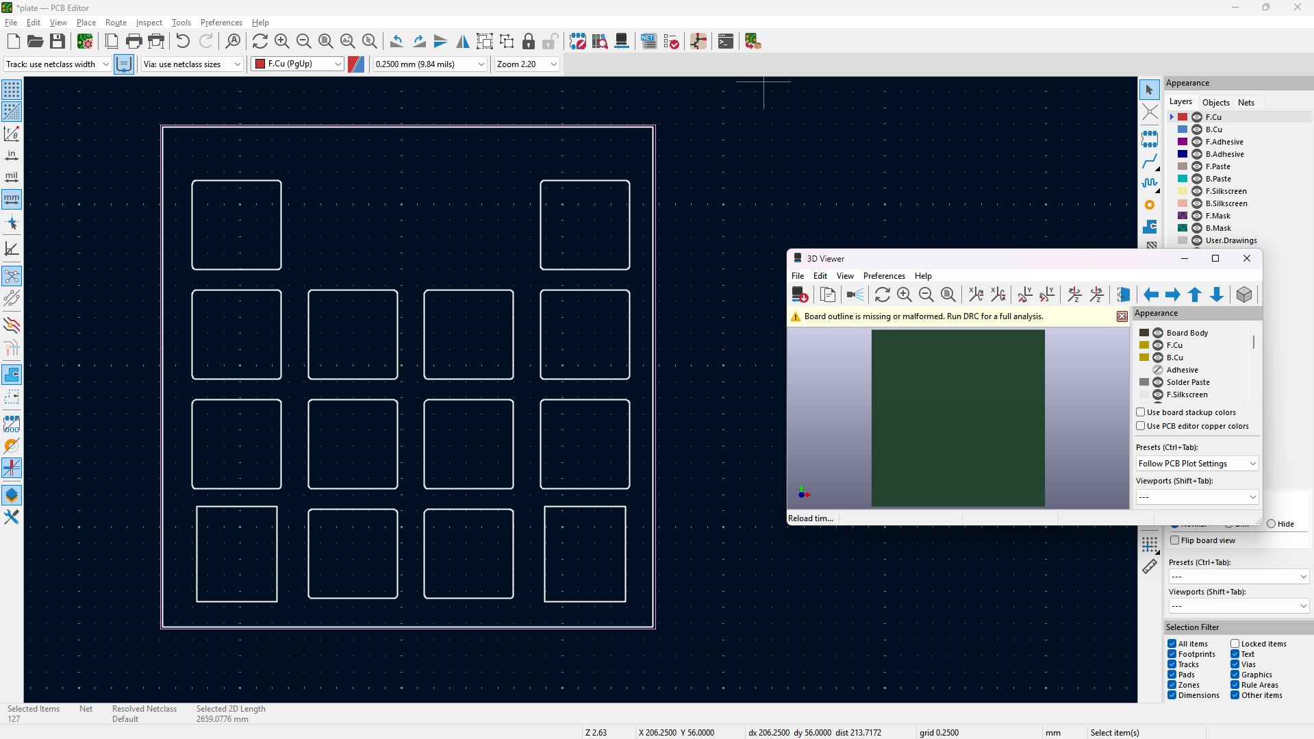
I JUST SPENT 5 HOURS TRYING TO GET THE DXF SKETCH OF THE PLATE EXPORTED FROM FUSION TO WORK IN KICAD... the whole time it gave the error below - malformed outline. WELL, it turns out even though IT fails to show the 3D model according to the outline, when exported with the Fabrication Toolkit, it works in JLCPCB 😭 (this was such a waste of time just for nothing).
Now I'm going to start writing the README etc.
[!NOTE]
Total time spent: 9h
21/07/2025
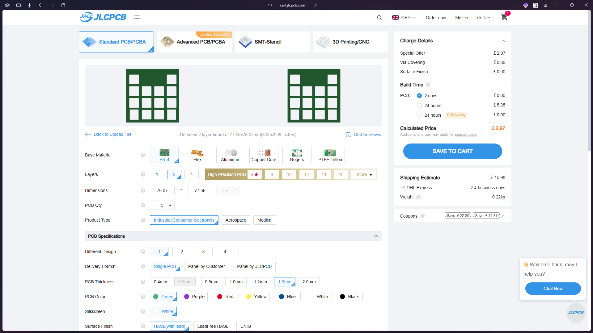
Redid the BOM to make it under the $150 limit, had to change some case parameters for that though (thanks to parameterisation it was easy).
[!NOTE]
Total time spent: 6h