
Tadpole FPV Drone
A small FPV drone that has a custom cost effective transmitter PCB.
June 6th: Drone Parts Selected + Work On Transmitter Electronics
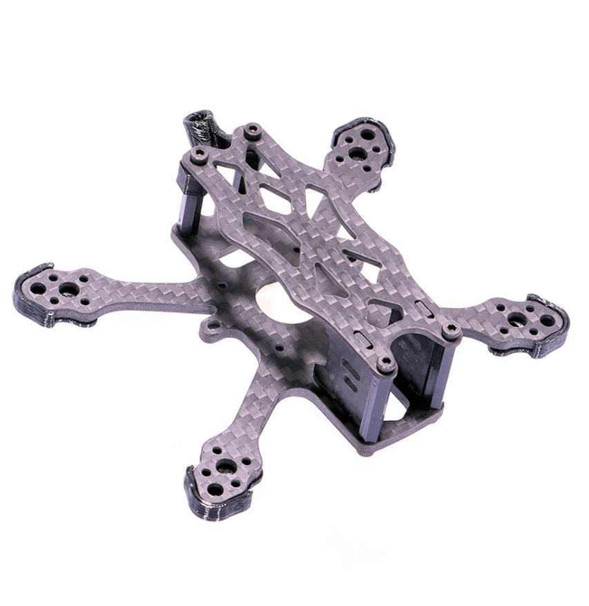
I looked around at some images prior to starting this project and decided I wanted my drone to have a smaller form factor, similar to a APEX 2" drone.
That inspiration frame looks like this:
After looking around at some other builds of this form factor, I found some similar parts that I could use and created a parts list in this google doc:
https://docs.google.com/document/d/1UYxp3Jcj_MZBELJUi8HEg_IUyJKEcsd3nflhL_p9VP8/edit?usp=sharing
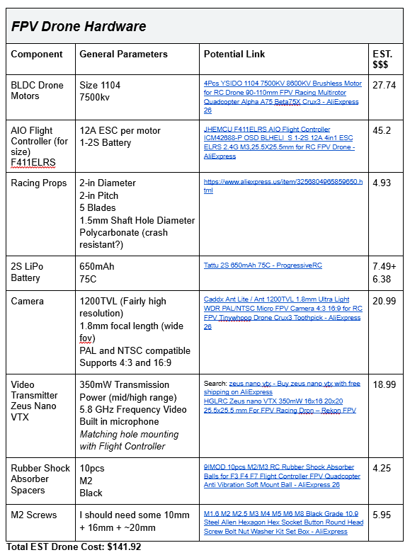
Finding good parts on AliExpress was more tedious then I expected as the prices seemed to keep changing, but I think I have a good completed list for the drone that should work well together.
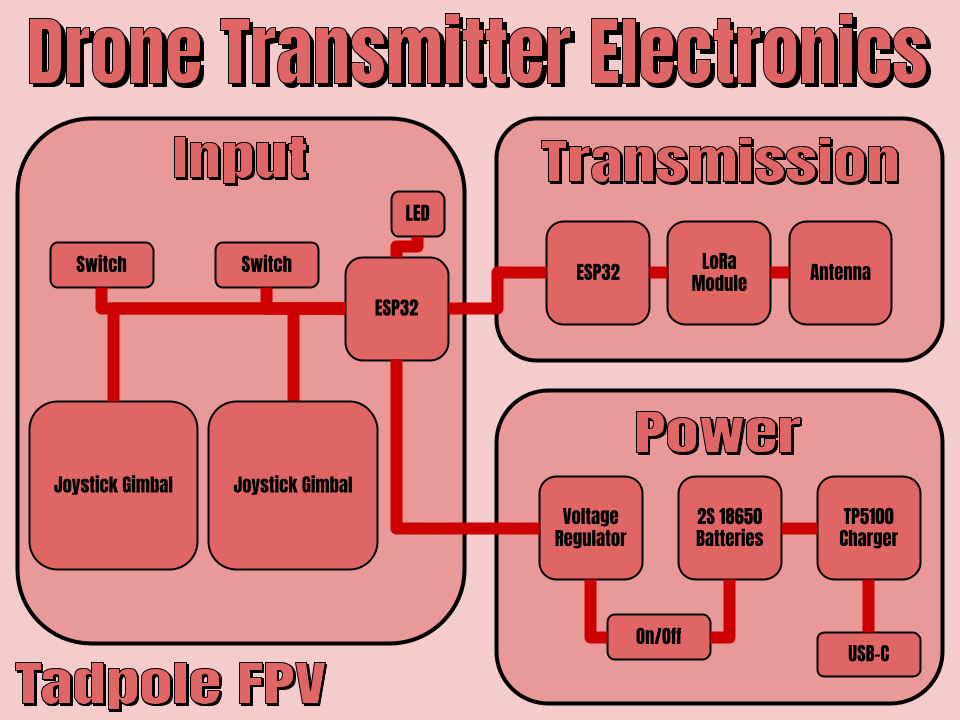
I also worked to figure out how I could control the drone with a custom transmitter PCB. I found that the flight controller I selected would work with ExpressLRS, which is an open source radio link protocol that would work with an ESP32 based transmitter. By pairing the ESP32 with an appropriate LoRa module I found, I should be able to create a custom transmitter PCB that can control the drone.
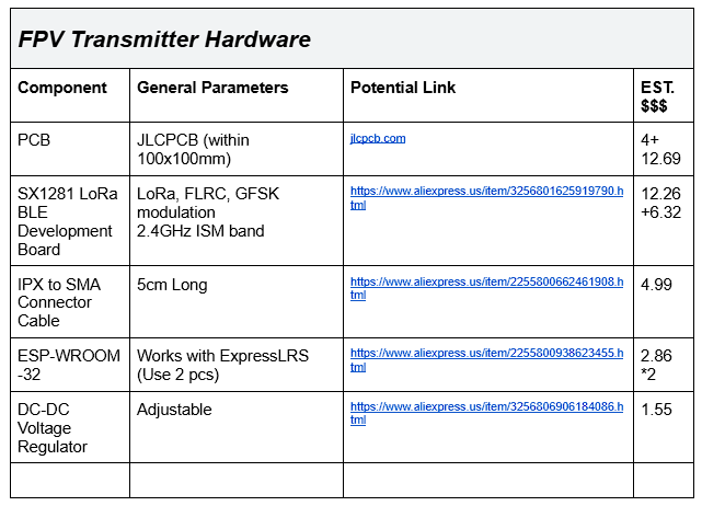
(The Transmitter Electronics list is still a work in progress)
Total time spent: 4.5h
June 21st: Back From Surgery! Finalized Transmitter Electronics
I had to take a massive break from this project due to a surgery I had, but now that I'm back I can continue working on the drone.
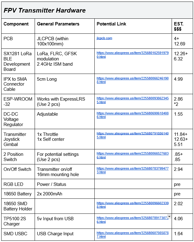
I figured out the final parts I would need for the transmitter electronics and found suitable parts on AliExpress. Once again, finding such parts with the specifics I was looking for was more time consuming than I was hoping for.
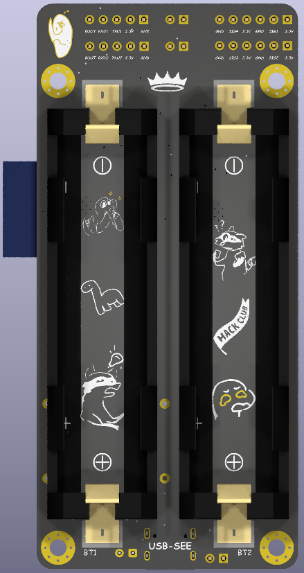
I wanted to keep the device charging as easy as possible so I am using USB-C for the power input and 18650 battery charging.
I also created a mockup of the transmitter electronics that I will be designing in KiCAD.
Total time spent: 4h
June 22nd: Started PCB Design in KiCAD
With the parts selected, all I needed to do was add them into KiCAD... Little did I know this would be the hardest part of the session.
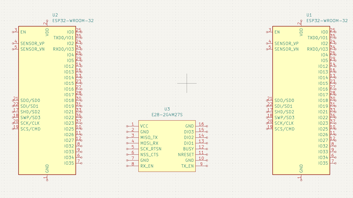
Finding all of the correct schematics and footprints for the parts was what I spent a good few hours on.
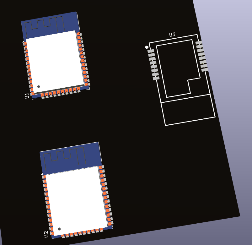
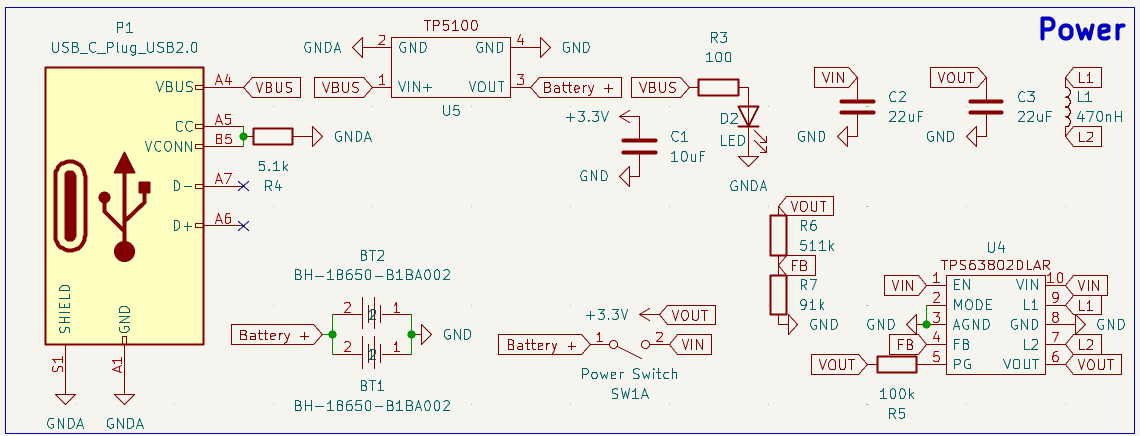
Eventually I had gotten the schematics and footprints imported correctly into KiCAD as shown by these glorious screenshots:
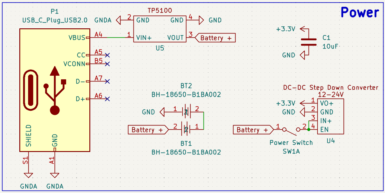
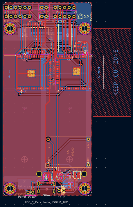
After getting these key components in, I wired up the schematic starting with the power section.
After getting the power section wired up, I moved on to the LoRa module and ESP32 transmitter section.
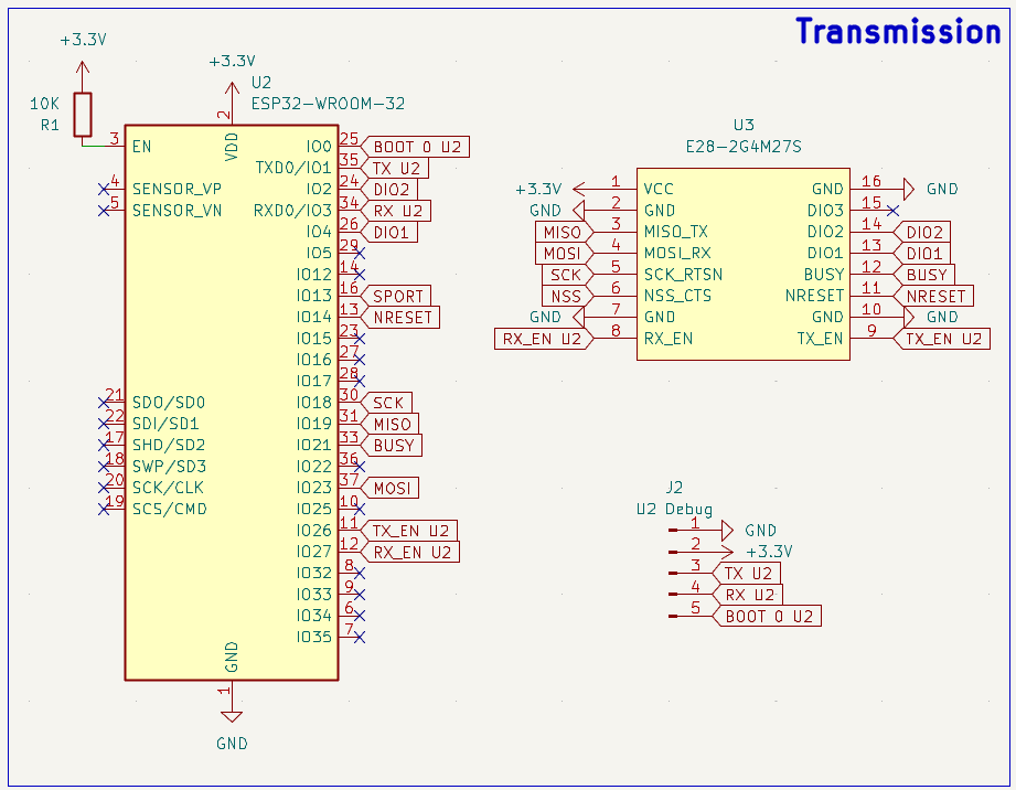
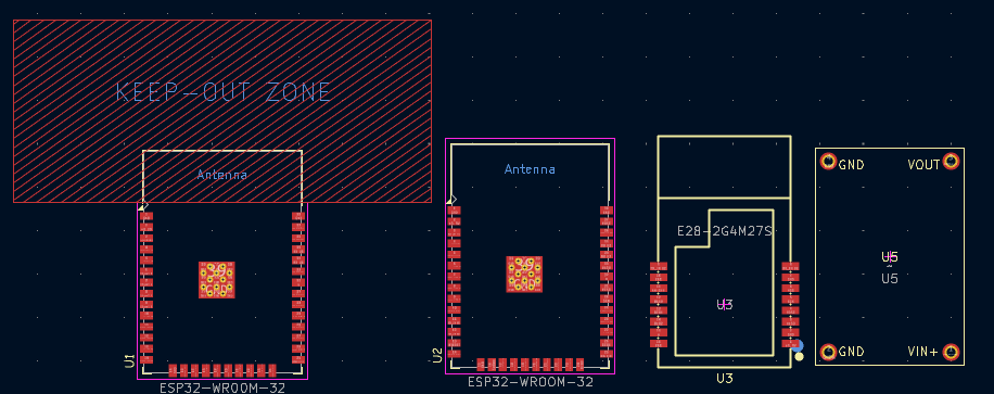
The last thing I worked on for the day was a custom footprint for the TP5100 battery charger as well as removing the keepout zone from the LoRa ESP32 module. (As it would not need to use Wifi or Bluetooth)
Total time spent: 5h
June 23rd: Finished PCB Schematic Design
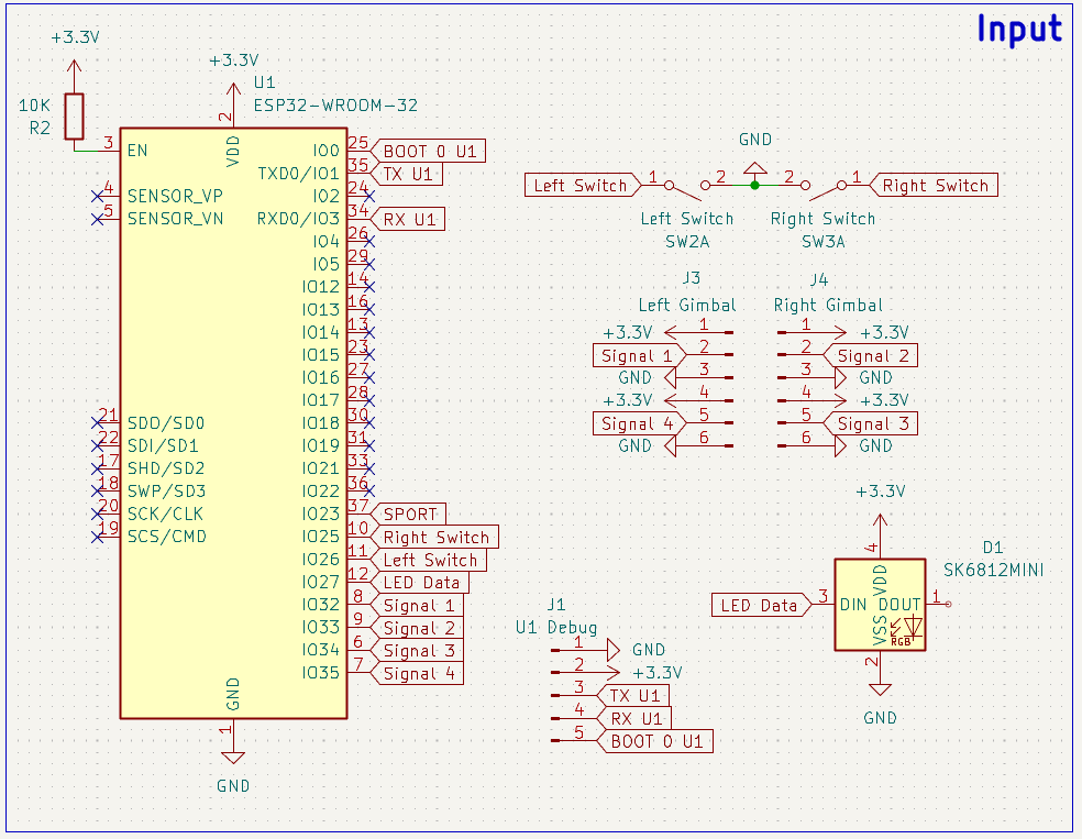
I finished up the input side of the controller by adding pins to interface with the gimbals and switches.
I also went through and added a footprint for each of the components in the schematic that didnt already have one.

No harm in double checking the footprints, right?
Total time spent: 2h
June 23rd: Wait theres a problem...
While looking over the schematic, I realized that I had made a mistake in the power section. Due to some interesting advertising, I had thought that the TP5100 battery charger could handle 2S batteries, but it turns out that is not the case. I elected to switch my batteries into a parallel configuration instead of series, which would allow me to use the TP5100 charger. This meant I had to change my buck converter since the new nominal voltage would be 3.7V instead of 7.4V. (The buck converter I had selected needed at least 6V to operate) Soon I was down the rabbit hole of finding a new buck converter that would be able to work with the new voltage.
During this process, I found the WEBENCH Power Designer by Texas Instruments, which I used to create a buck boost converter schematic that would work with the new voltage.
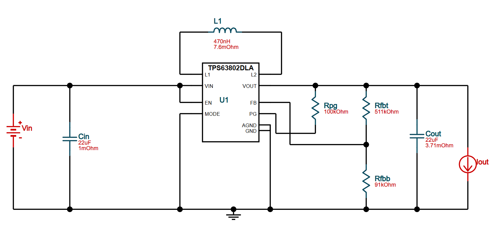
I also found some components on LCSC for the schematic.
Total time spent: 2 more hours...
June 24th: Finished PCB Schematic Design (Again)
Figuring out how to import all of the components from LCSC into KiCAD quicker this time. The issue was that it did it in a kinda weird way, leaving me going around in circles trying to figure out how to actually get the parts into my schematic.
Anyway, I got the parts imported and added to the schematic and wired them up.
The next challenge was figuring out the footprint naming conventions for the parts.
imperial vs metric woes...
After I did this I was able to update all of the footprints to be the correct, cheap, smd components. (Soldering this later will be fun...)
At this point I should be ready to finally start the PCB layout :p
Total time spent: 3h
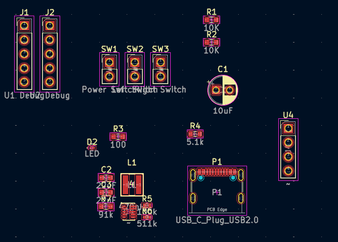
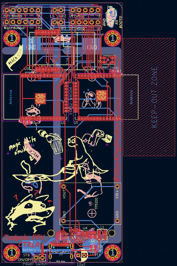
June 25th: Finished PCB Layout and Wiring
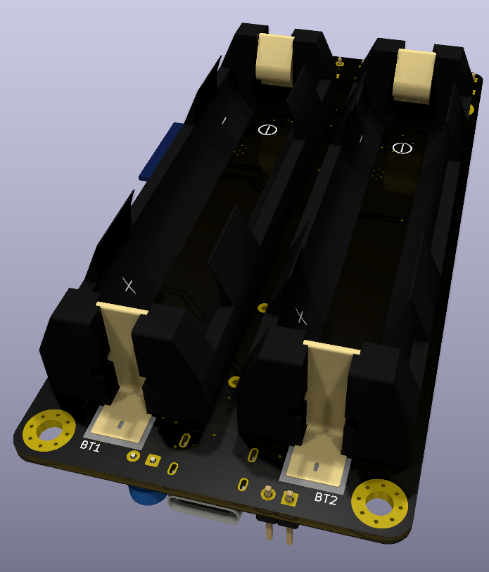
I started the day knowing I wanted to make the PCB as absolutely small as possible, and portrait.
The size would be largely constrained by the battery holders on the back of the PCB.
Placing components got interesting as the batteries prevented me from adding tht components in that area.
This meant that a majority of the components would get pushed to the extremes of the board.
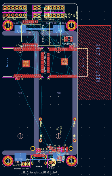
With all the components in place, I started wiring the traces of the board. This process was made harder by my incessent love of thicker traces, and close component positions.
Now this is my kind of puzzle
I used .4mm traces for a majority of the board leading to this quite mesmerising power section routing:
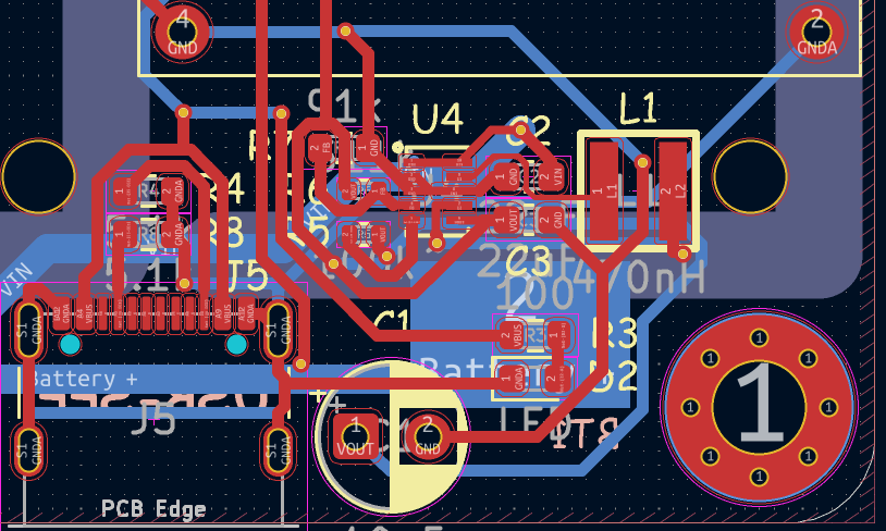
After a good while with some music in the background, I reached this:
Total time spent: 5h
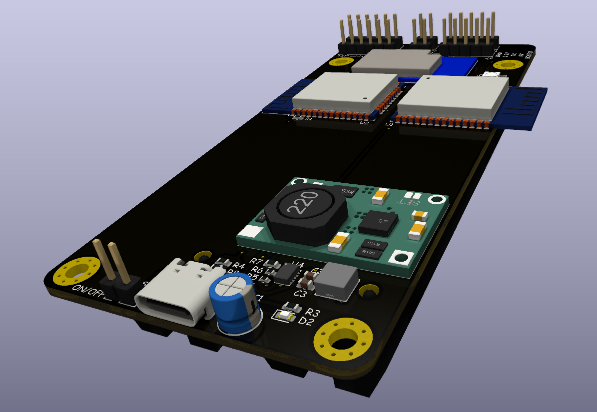
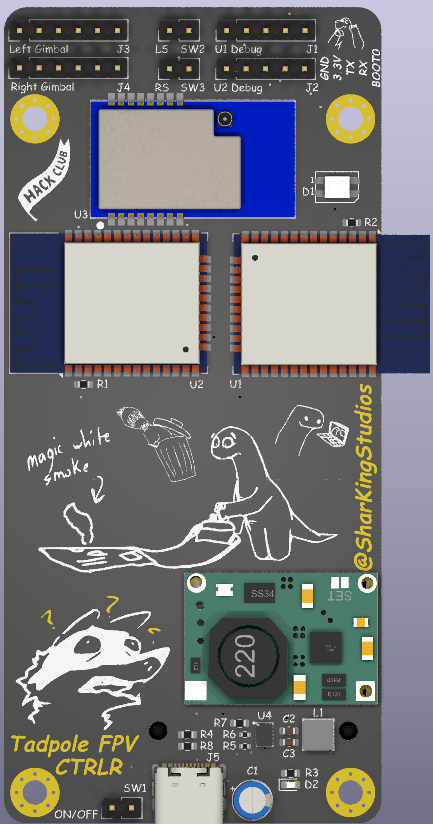
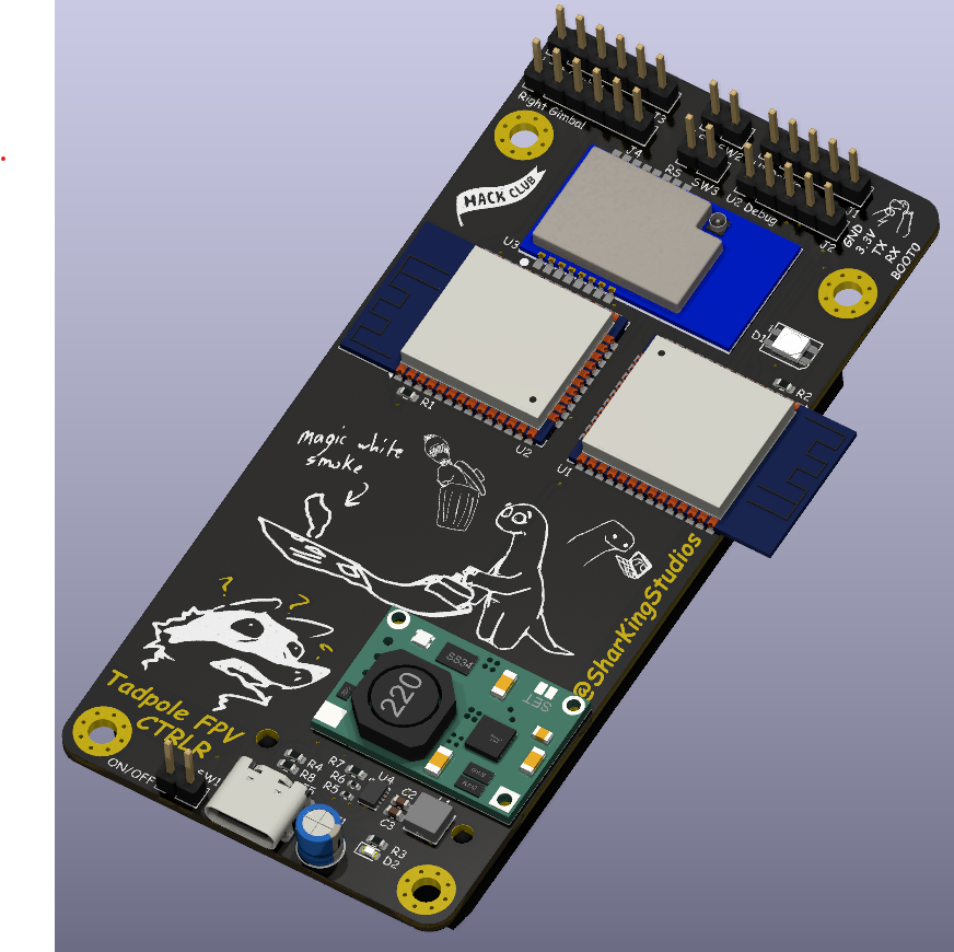
June 26th: PCB Art!
I spent the day working on the PCB art and getting it ready for fabrication.
Here's the latest renders of the board:
Total time spent: 2h