
Meko Pcb
9/30/2025 - Looking for an SoC that has bulilt in USB controller
V1 had a few issues, one of them that there had to be a whole separate chip to convert from usb to uart for the esp32 (gen 1), and in general it is kinda hard to flash a first gen esp32.
But the problem is that from my research the only SoC that has Bluetooth audio, and wifi is the first gen esp. So v2 probably won't have Wi-Fi, so no Spotify/other streaming. Which is kinda sad, but I rather have a less feature packed project, then a project that is not in a working condition like v1.
So far I have landed on the STM32WBA65CI, it has ble 6.0 and audio support, its beefy, has plenty of io, and most importantly an integrated usb controller. Maybe for a next version I will add an esp32c3 has a Wi-Fi module, but first this has to work
Also, some other stuff that I have been thinking on changing/leaving for v2:
- I will not use 0402 components, and other small components in general, it's just a pain to debug and work with, once I have a working prototype, I can do a version with small components
- Simplify the power and battery systems, I won't use a power path and a fuel gauge chip, just a tp bms and a voltage divider for the battery percentage
- I am leaving the DAC/AMP chip, and all the surrounding circuitry, except I'm using larger package sizes for the accompanying components

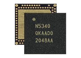
10/8/2025 - Realized that the nrf5340 exists
Realized that nrf has much better documentation, more examples and a better rtos. It has less ram than the stm32, but it is much more power efficient.
I have worked with the nrf52840 before, and it is almost the same. I'm just worried about routing the second row/layer of pins on the package
10/15/2025 - Found my dream BMS
I just found out that Nordic makes BMSs specially for the nrf5 series, it's called the npm1300, so they have full example schematics of the two working tougher!! It also has fuel gauge functionality, and is able to monitor every voltage in the system. It has two voltage regulators built in, that you can also control with i2c. It has native support for USB power negotiation. It also seems pretty easy to implement.

Most of my devlogs so far have been doing research😭
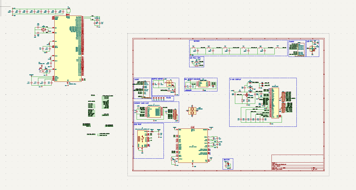
10/16/2025 - Started to redo schematic
Deleted a whole bunch of components. Added in the nrf5340 and all of its surrounding circuitry. Also added the npm1300, I'm so excited to use this bms btw (≧▽≦) removed the old BMS, some of the regulators, because the BMS has built in ones. IDK if I should use 1.8V logic or 3.3V logic though
10/20/2025 9 PM - Reread the datasheet of my AMP/DAC chip
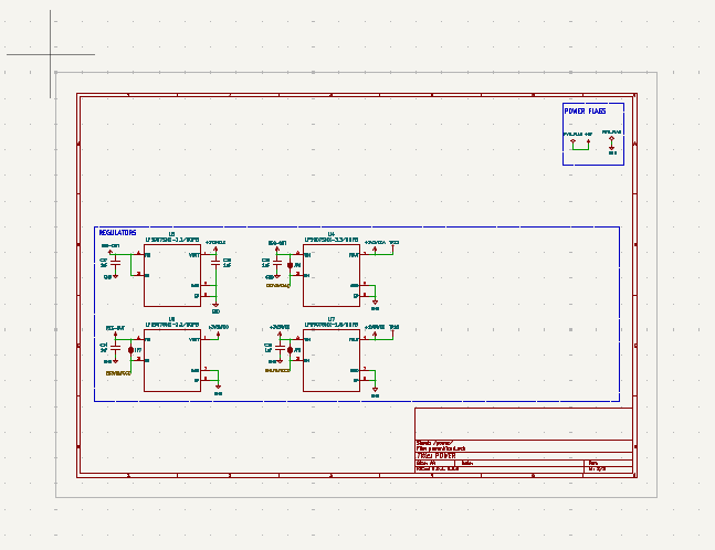
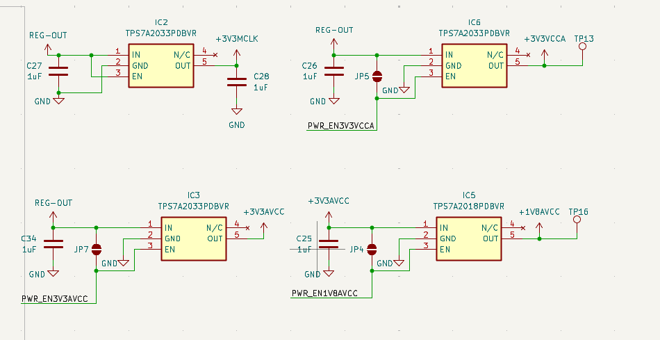
In v1 i used 1mm1mm power regulators for my audio chip, which were hell to debug/hand solder. SO this time I'm using almost the same regulator from TI, but in a 3mm3mm sot-23-5 footprint. I reread the datasheet of my audio chip, and realized that I don't actually need one of those regulators, so I'm now two regulators down, the other that I removed was my general 3.3v regulator, because the npm1300 has one built in.
Also, my hall effect sensor for my dial draws a lot of idle current, so I utilized one of the load switches of the npm1300(my beloved) to no give power to it when the device is in sleep mode
10/20/2025 11 PM - Finshed rough shematic
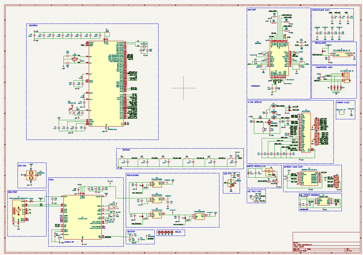
I finished the power train. Connected everything to the soc. Removed/separated a bunch of nets from v1, where I was in a shortage of pins, so i combined reset pins and similar things. Switched over to spi from sdio for the sd card. Made the schematic prettier
10/21/2025 - Many small changes
I went over the schematic again, fixed some stuff.
I used mouser for v1, and i plan to use lcsc for v2, so i replaced the parts that lcsc doesn't have, except my amp/dac, I will solder that to the PCB using hot air reflow. Furthermore, I also moved from an externally powered oscillator to a plain old crystal for my dac, it's just simpler this way. Changed footprints from 0402 to 0603 for better debugging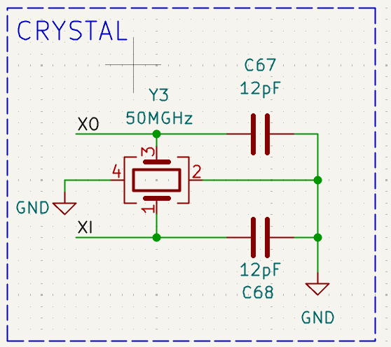
10/26/2025 - Switched out DACs
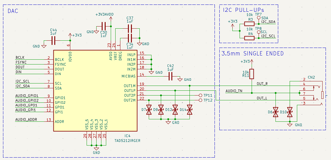
I posted my design on the kicad discord for review, and the people there pointed me in the right direction about my DAC. The ESS DAC that I was using was expensive and hard to implement, I switched to the TI TAD5212 which has the same performance, and is a lot easier to implement, and has a bunch more features, and it's half the price at $5, and it's also available at lcsc, so I can get PCBA.
I spent a lot of time reading the datasheet
I also switched out some parts from v1 that were not available at lcsc that are available.
The schematic is almost done, the last thing i might add are some charging indicator LEDs to the pmic.
10/27/2025 - added leds to the pmic
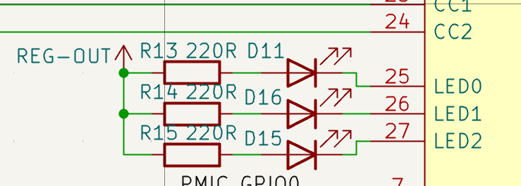
Made final touches to the schematic, added leds to the pmic, double-checked everything one more time. Added some more testpoints, but i will add a lot more.
I'm debating doing double-sided pcba, but IDK if I will fit in the budget
10/28/2025 1 AM - Chat I might be cooked
My pmic is not available in a qfn package at lcsc, only in bga😭 First bga that I will use every, so I watched a bunch of altium academy videos about bga design. Also I need 0.2/(0.3)mm vias for both the pmic and the nrf53, so 5 PCBs will cost around 69$ (nice). I also checked how much would double sided PCBA will cost, it's around 210$ USD for two PCBs. So tier 1 here I come!
I'm pretty scared that this won't work like V1, so I'm putting extra effort in to quadruple-check everything. I will also place a frick ton of test points.

10/28/2025 11 AM - Rethinking how to make this prototype PCB
I was worried on the size of the pcb, make it as small as possible. With V1, this came to my demise. In v2 the main goal will be to be able to fix mistakes that I made, so I will leave spacing between components, put a bunch of test pints and bridgeable/cuttable test pads, and not worry myself about the size of the final product. If this prototype works, I will shrink everything down for production.
I'm also reconsidering the nrf54l, which is available in a qfn package, but most likely I will stay with the nrf53
10/28/2025 8 PM - Added a butt ton of testpoints
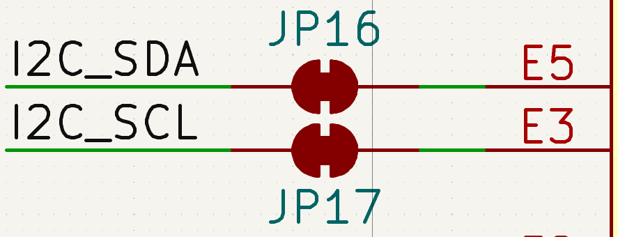
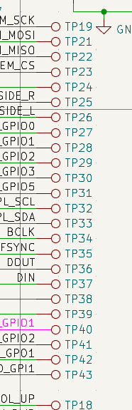 I also added a bunch of jumper pads on the i2c lines, so i can isolate one component if i want too. In the same way I also added jumper pads on the power of the chips, so i can just disconnect them
Im staying with the nrf53, because the nrf54l doesn't have audio pll, so small vias it is
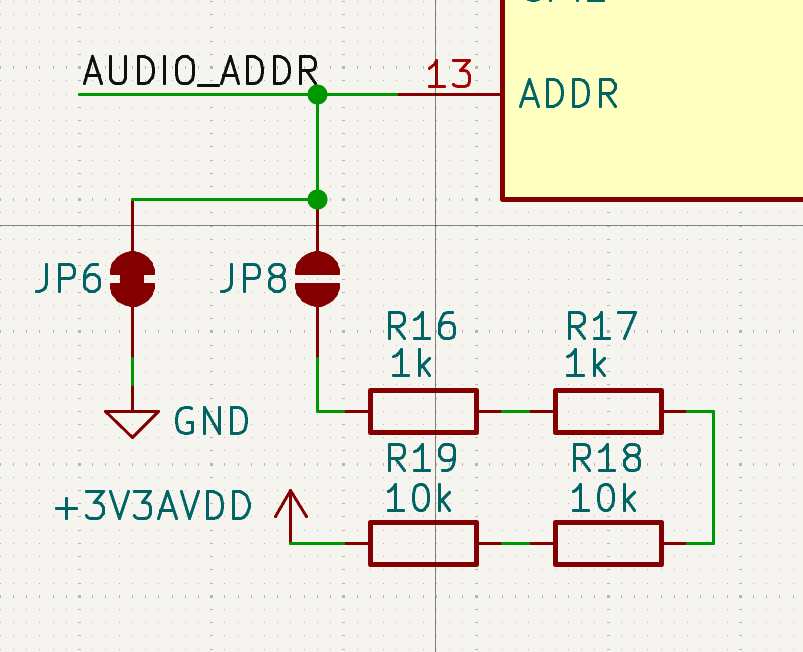
I found a bug, I connected the i2c address pad of the dac to a gpio, now i have two options for and address
10/28/2025 10 PM - Changed out the parts that were not avalibile on lcsc


I still had some parts that were not avalabile on lcsc from v1, so i looked for new parts, I changed out the usb port, display fpc port, vibration motor
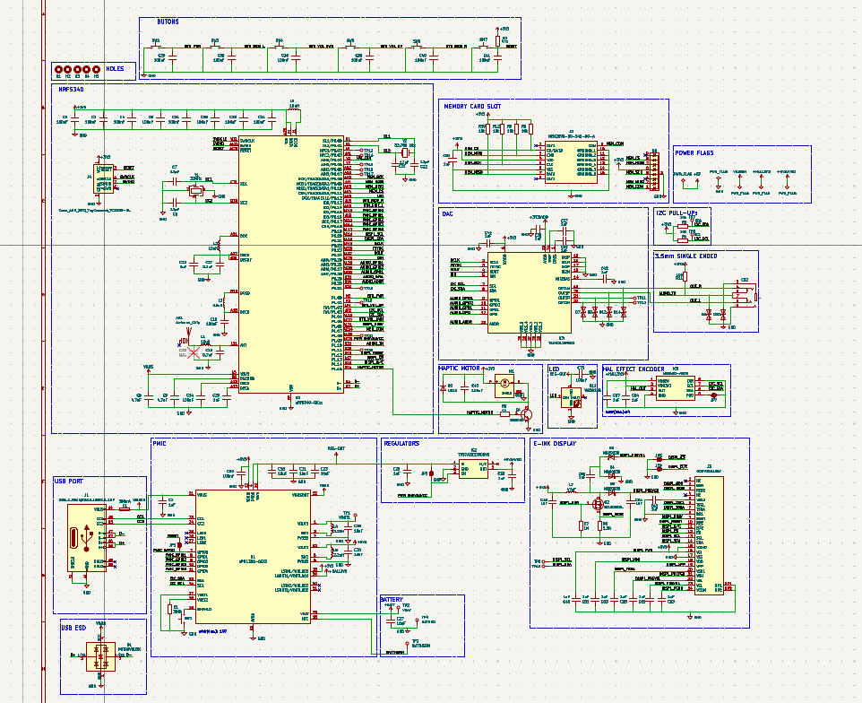
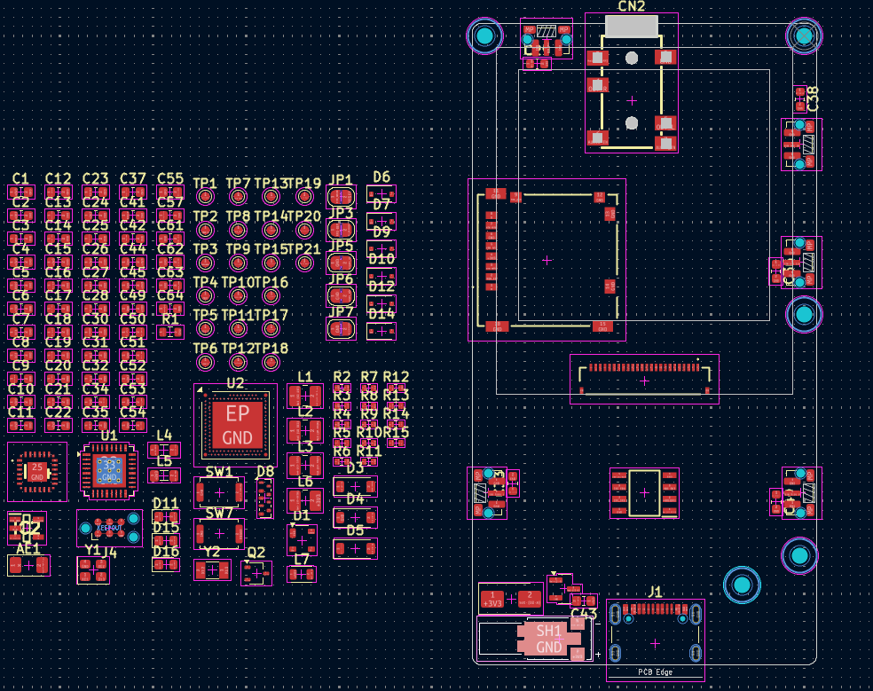
11/5/2025 - Almost finished with basic layout
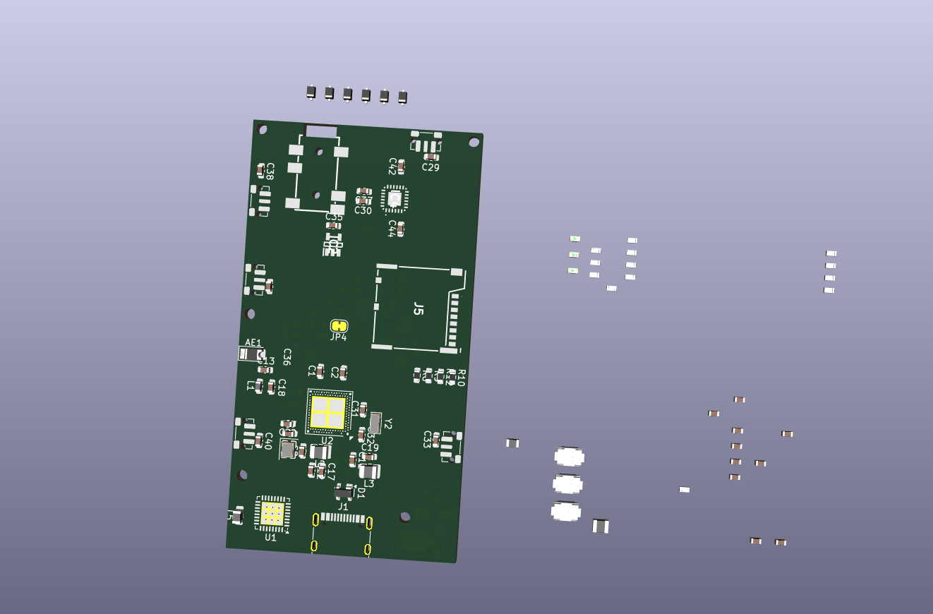
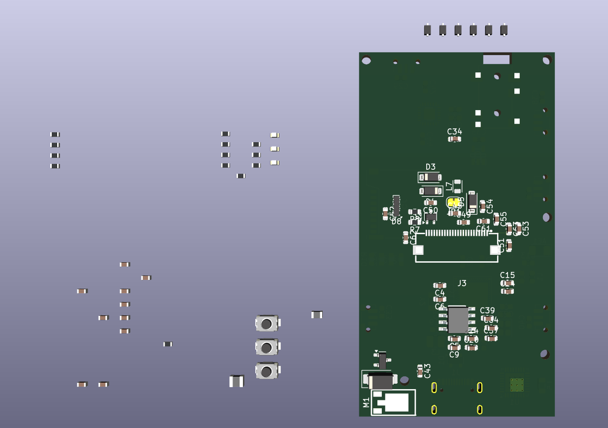
This is a rough layout, just to help me visualize how I should proceed
Still contemplating using a module for the nrf53, seems easier, and if i want to sell this later on i wouldn't have to get rf certification
11/6/2025 - finished first pass of rough layout
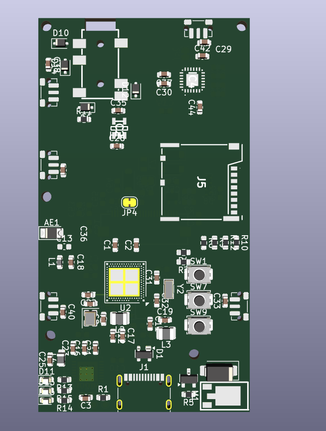


i still need to add 3d models, and place all the testpoints, some jumpers and the swd connector
I will stay with this package i think, it will be fun to be able to use small vias like ts