
In13 Spectrum Analyser
Total: 25 hours
Sunday 18 May (2hr)
I started to do initial research and then I begun to build a schematic.
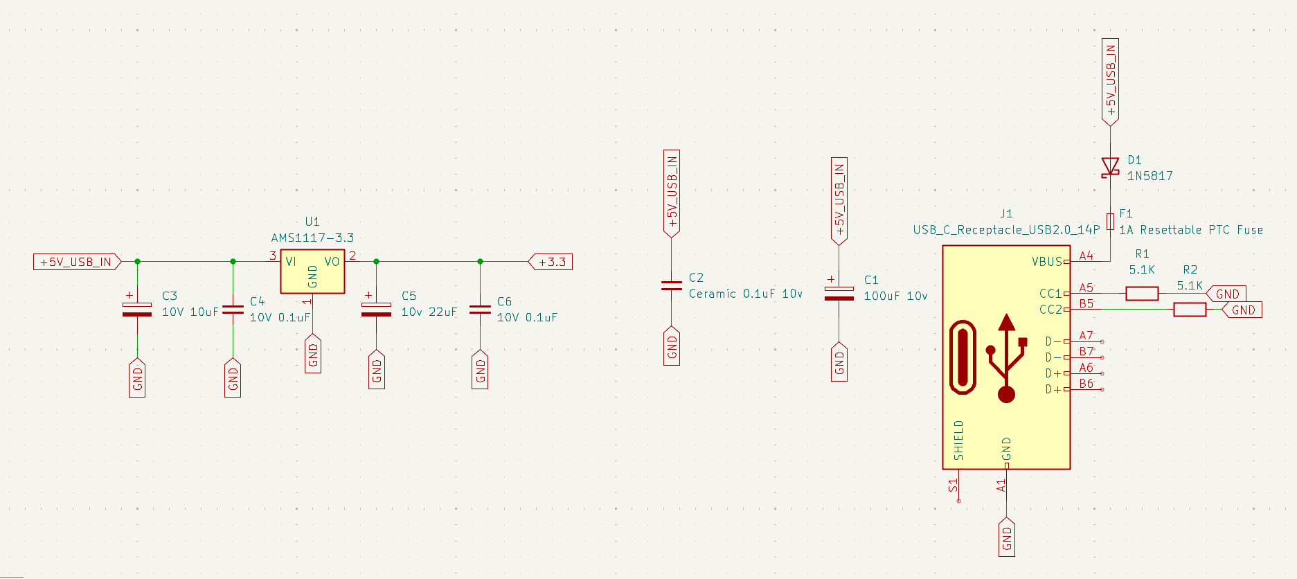
I started by adding a USB-C port. This port has the 5v input and ground. Pins CC1 and CC2 are both connected to ground with a 5.1k resistor. This allows me to tell the power source that I am requesting 5v power as a legacy device.
I then added a decoupling capacitor between 5v and ground to smooth out the 5v supply. I also added a 0.1uF ceramic capacitor to perform High frequency decoupling on the power input. I added a resettable PTC fuse and Schottky diode to perform protection on the input and reverse polarity protection. I used a Schottky diode to minimise voltage drop.
I then added a 3.3v regulator to create a 3.3v rail for the ESP32 that will process the audio input. I chose a low dropout regulator and connected the inputs to my 5v system. I added a 10uF input capacitor to the input and a 22uF output capacitor for voltage smoothing. I then added 0.1uF ceramic caps to the input and output to perform high-frequency decoupling.
Monday 19 May (2.5hr)
I researched how to spit my audio output into different channels. I ended up choosing a MSGEQ7 chip which splits the input audio into 7 bands.
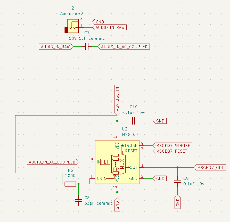
I start by taking the output from my audio jack and adding a coupling capacitor in serices to remove and DC offset from the audio signal, this is because the MSGEQ7 expects an AC audio signal. My design expects a line level input from an audio jack.
The reset and strope pins of the MSGEQ7 are connected to labels to be controlled by the ESP32. The output of the MSGEQ7 get given to an ADC on the ESP32. An external capacitor has been added for the oscilator in the MSGEQ7. An output filter capacitor has been added to provide stability to the output and a decoupling capacitor has been added to decouple to power supply.
Monday 19 May (2hr)
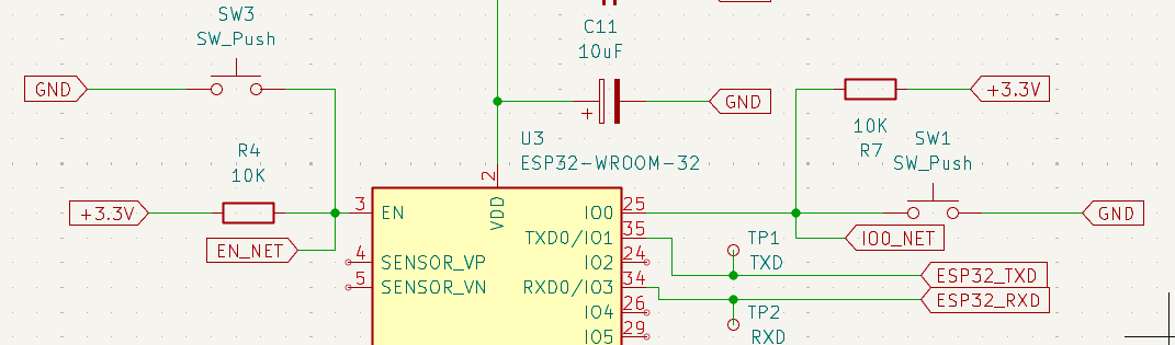
I added the esp32 control board here. I chose an ESP32 WROOM 32 dev module.
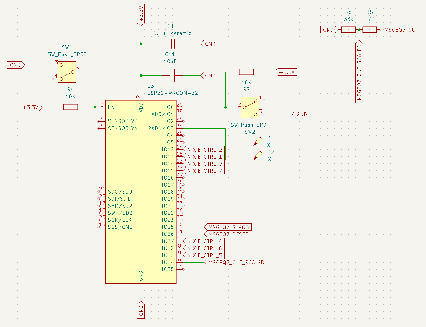
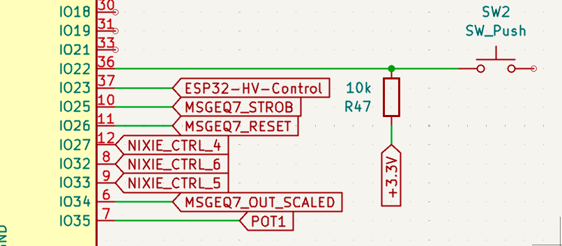
I started by powering the ESP32. This chip uses 3.3v and is therefore powered by my 3.3v rail. Ground is connected to my common ground rail. The EN pin is pulled to high with a button to connect it to ground and act as a reset button. I have 2 decoupling capacitors, these are an addition to the decoupling capacitors inside the model but can't hurt so why not! The MSGEQ7 output is connected to an ADC input with a voltage divider to bring the 0-5v signal down to a 0-3.3v signal. The strobe and reset pins from the MSGEQ7 are also connected to the ESP32 so they can be controlled via software. The 8 nixie tube control pins are connected to PWM capable outputs on the ESP32 to allow for dimming. The TXD and RXD pins are connected to test points to allow for flashing of firmware. the IO0 pin is pulled down to GND by a button to enter flashing mode and is conencted to +3.3v via a pull up resistor by default.
The ESP32 can be flashed from the test points using a USB-to-Serial converter.
Monday 19 May (3hr)
I created the driver circuity for the nixie tubes. This has been done assuming the 140v is on the +140v rail (I will add this circuitry later).
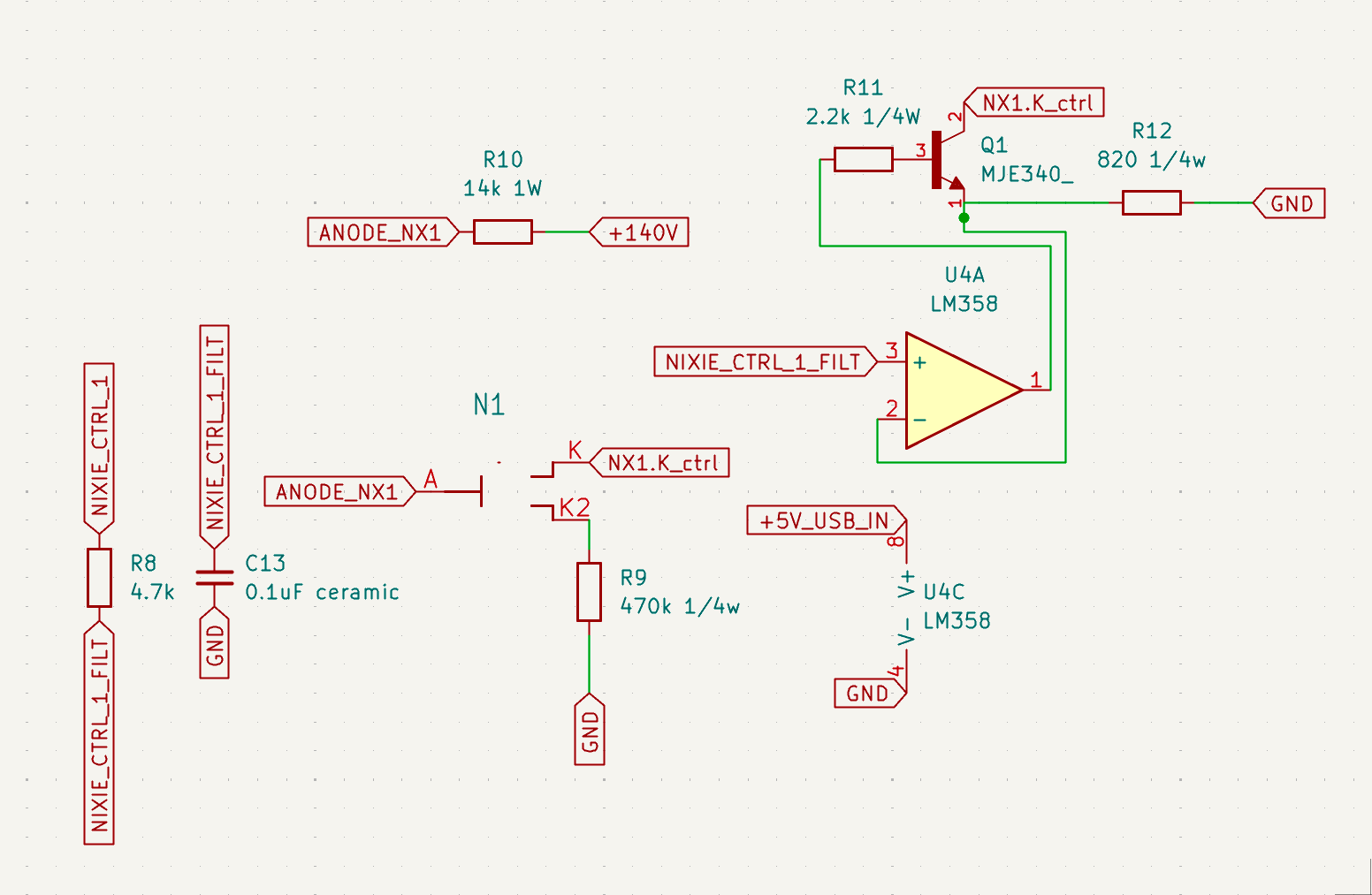
I first created a low pass filter for the PWM Smoothing converting the PWM from the ESP32 into a smooth analogue voltage. I have a 4.7K resistor from the nixie control pin to create this low pass filter. I have also got a capacitor from the filtered output to ground as a minimum cut off. I have added my nixie tube and connected the control to the collector if the driver transistor and the aux to ground via an auxillary cathode resistor. The annode is connected to 140v via a 14k resistor. I have used an op-amp to buffer the nixie control frequency and drivbe an NPN transistor. I am using a high voltage NPN transistor. I also have a base and emittor resistor connected to the trnasistor. The emitter resistor sets the relationship between the nixie control output and the current in the cathode.
I then duplicated this design 7 times (one for each tube), changing the labels accordingly.
Tuesday 20 May (3hr)
I created a power supply to boost my 5v to 140v to power the nixie tubes.
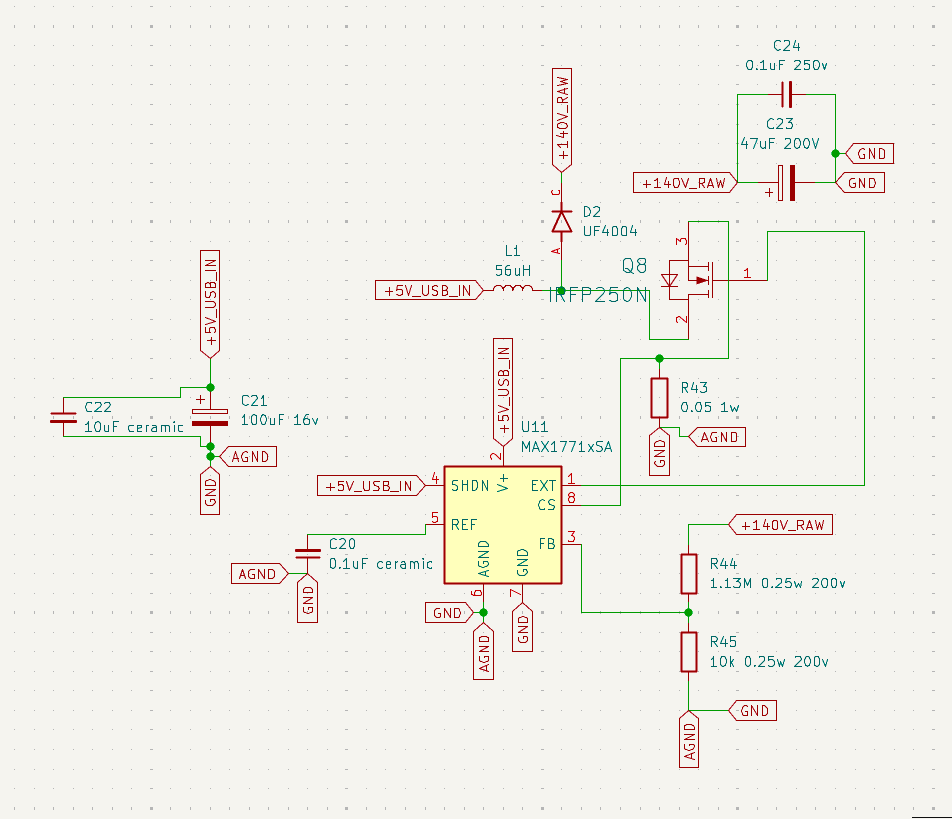
To create my 140v line, i am using a MAX1771 IC. This IC is commonplace on many nixie tube power boards and is therefore the obvious choice. I have performed input decoupling on the 5v power for the high voltage section. I am using an N channel mosfet which is driven by the MAX1771. The MAX1771 turns onm the mosfet allowing power to go through the inductor and through the mosfet to ground. The inductor opposes the change in current causing the current to ramp up linearly over time. The inductor stores its energy in its magnetic field. The diode is reverse biased during this phase, so no current can flow through it. The output capacitor is supplying current to the nixie tubes during this phase.
The MAX1771 turns off the mosfet. The current cannot change in the inductor instantaneously, this means the inductor tries to maintain current flow. The indyctor then reverses its polarity, the reversed voltage addes to the input voltage creating a higher voltage. The diode becomes forward biased allowing current to flow from the inductor to the output capacitor. The inductor then ramps down its current linearly. This cycle repeats to create my high voltage.
Tuesday 20 May (1.5hr)
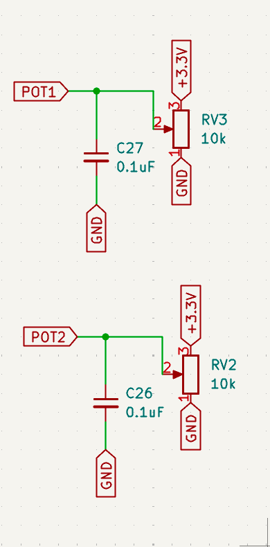
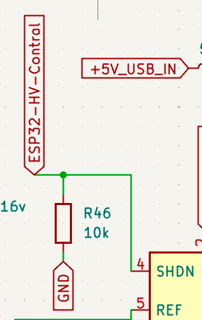
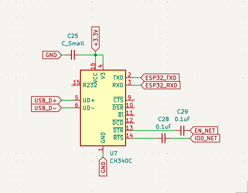
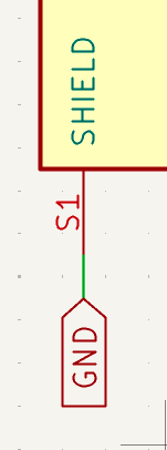
Small Changes have been made. I have added 2 potentiometers for volume and brightness control. I added a shutdown button and linked the shutdown rail on the MAX1771 to the ESP32 to allow it to shut off the high voltage when not in use. I have also done general schematic cleanup and I have added labels for readability. I also added a serial controller to allow me to write to the ESP32 through the USB-C port. I used a CH340C due to the minimal extra circuitry needed. I also grounded the USB-C shield.
Wednesday 20 May (5hr)
This was my first attempt at routing the PCB
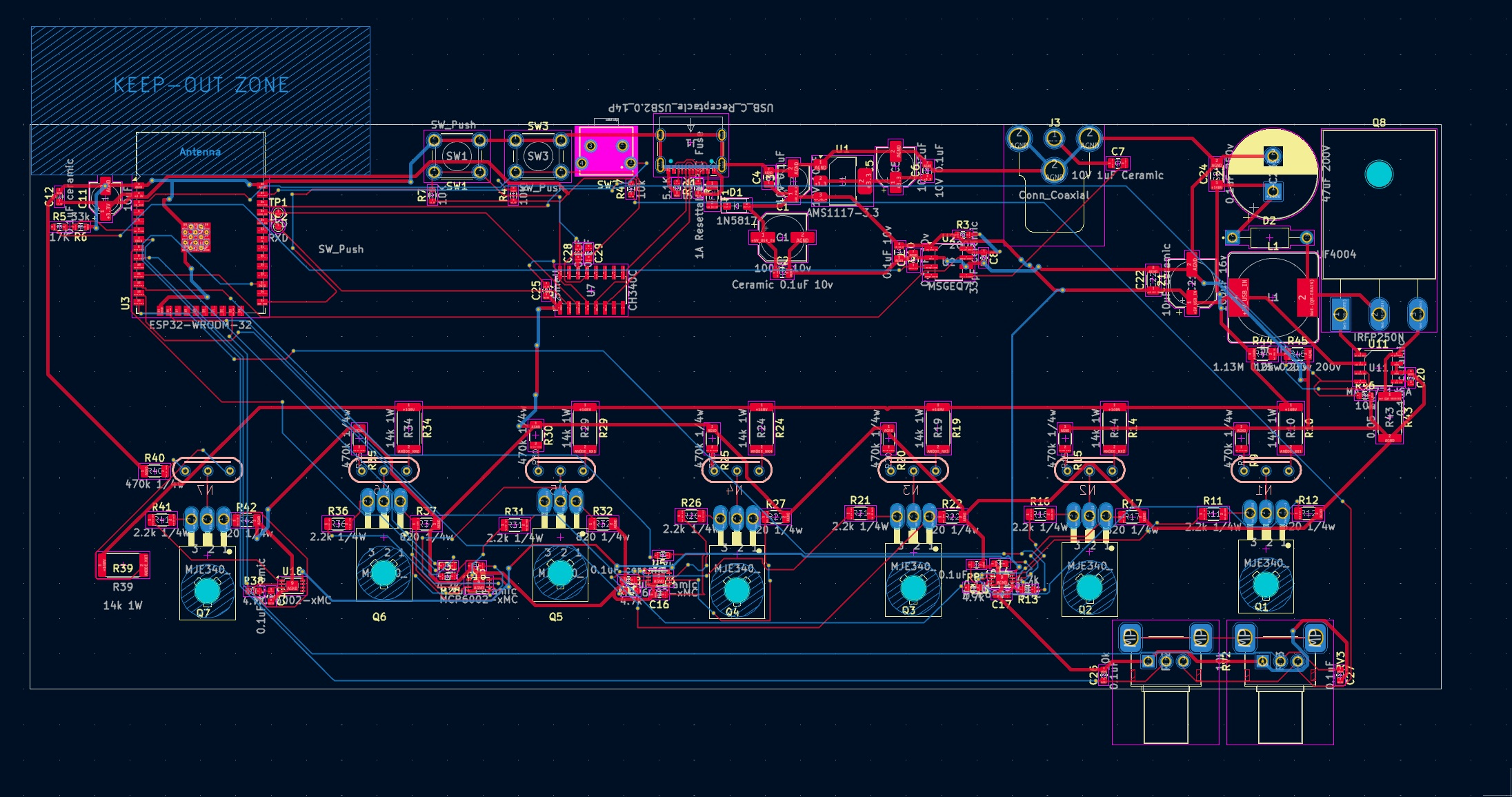
I learned from this first attempt that a ground plane would be invaluble. This proved my PCB was possible to route on a 2 layer PCB. Next time, I will make my PCB longer and use the bottom layer as a ground plane. I have my tubes on the bottom layer with electronics on the top to allow and large components to face down giving me more flexibility in my case design. In my next iteration I will also add mounting holes and rounded edges. Finally, I will attempt to use the freerouter autorouter on my next iteration with a new pcb layout.
Thursday 20 May (4hr)
This is my second (and hopefully final) attempt at routing the PCB.
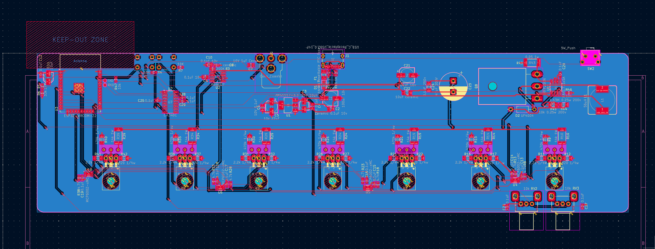
For this attempt, I used a ground plane on layer B to make routing easier. I also made the PCB longer to make it easier to route and to make the final assembly look better. I used freerouter to route this attempt as it gives a more optimised attempt than my manual attempt. After optimising the settings, freerouter was able to optimally route my PCB. I had to manually route my ground traces to the ground plane as freerouter does not support this automatically.
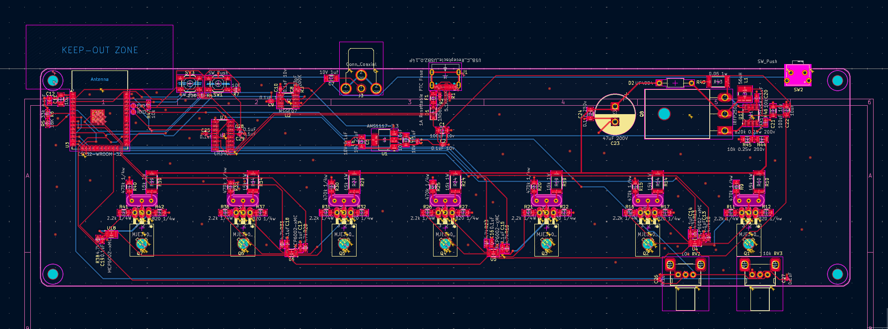
Wed 28 May (2.5hr)
I have added a second ground plane to the top of the pcb. I have also added standoffs to the corners. I have cleaned up the schematic.
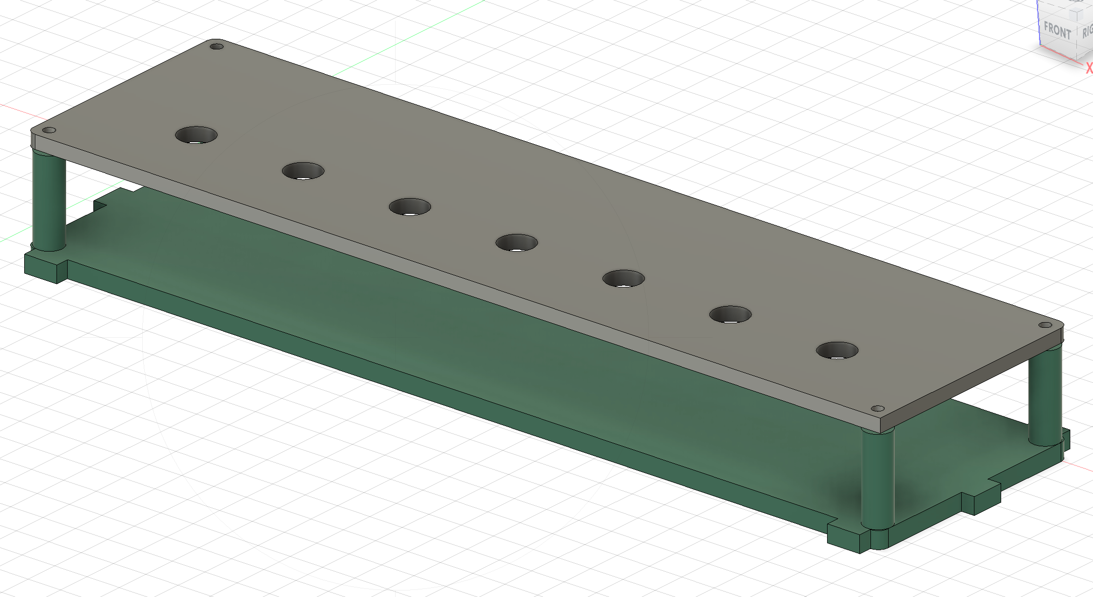
I designed a case for my model using a combination of laser cut and 3d printed parts. My case uses a laser cut kerf bend to allow the sides to be cut as a single piece and then this piece can be wrapped around.
Added readme.md

Wed 28 May (2.5hr)
I replaced certain footprints with ones available at JLPCB and re-routed.
Sun 1 June (1hr)
Added code for basic functionality and add mounting holes to the case to remove the need for glue.