
Train Locs Board
Train Locs Board
04/06/2025 & 05/06/2025
This is going to be a little LED train status board, This will show the Operating Company of a train whenever it gets into the station on the UK Midlands Mainline
Design
I think my basic design guidelines, electronics wise are: - ESP32 based board - USB C - As big of a RGB led as I can find
As far as design, I want to set a few constraints: - Show every station - Have an LED for every platform - Use the National Rail Darwin Real Time API to get platform status - Properly represent the physical layout of the network
Physical Design
I think I want to go for a single board design, This is due to the reduced costs of only needing 1 set of boards and 1 stencil. It also has a few other benefits, namely: - Easier to design, as no need to allign the connectors - Cleaner - Less fastenings are required (makes it cheaper too)
However, It also has a few downsides: - It makes it harder to design other track layouts - If there is a big issue in the board, it means all the components are wasted, not just the display or the controller.
Choosing Some Parts
Now we get to the fun part wink.
WS2812B
I started off by going looking for the biig neopixels, so I started looking on LCSC:
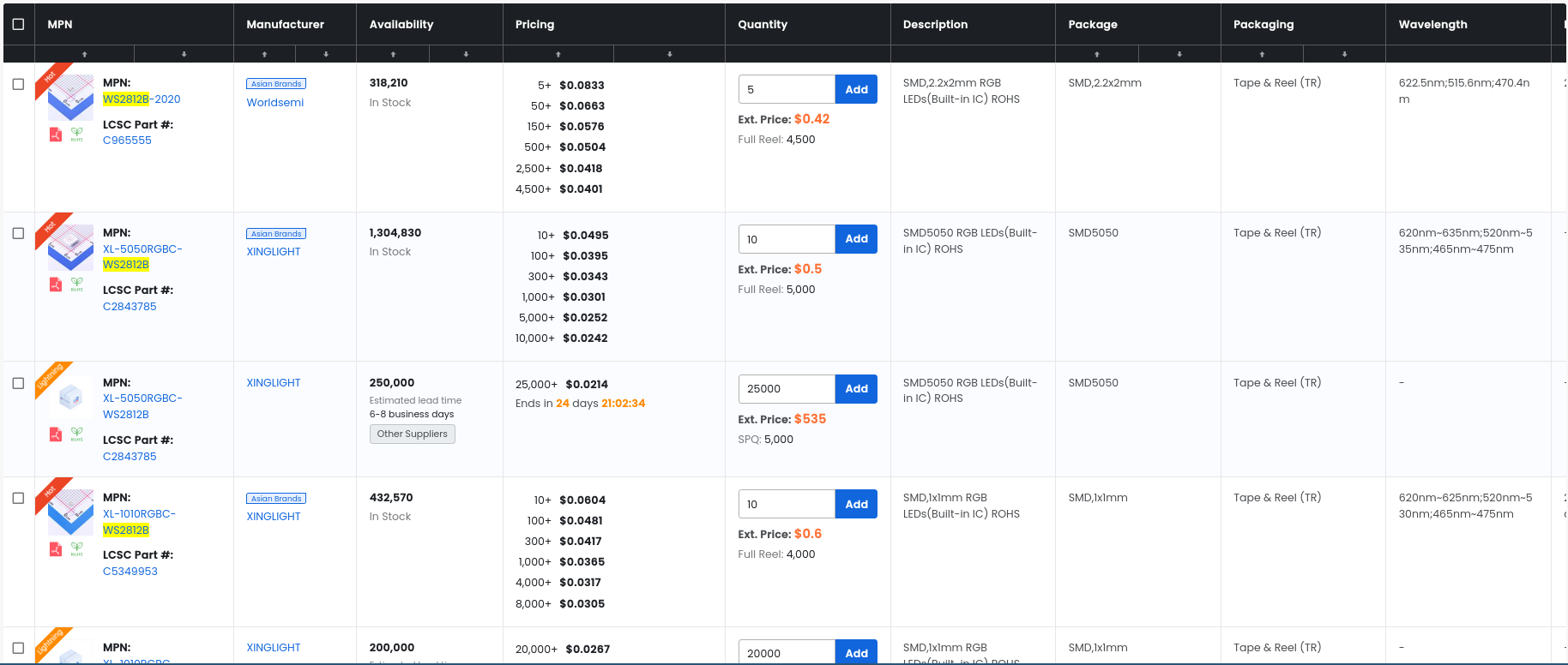 As you can see, there is a wide selection of sizes and other details, so I selected the descending filter and had a look:
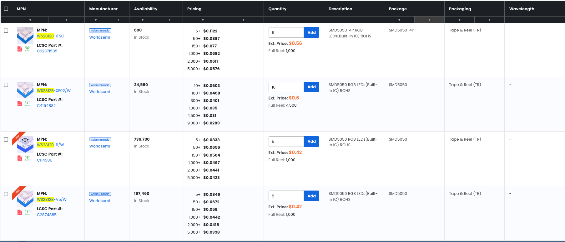 As you can see, the SMD5050-4P package is the largest, physically it's 5mm x 5mm. It is also relatively affordable at $0.1122 per unit (in orders of 5, I suspect it'll go down).
ESP32
Now to choose the heart of the operation, The ESP32. My requirements for this were simple, it needed to do 2.4Ghz WiFI as my IOT network is 2.4Ghz only. Otherwise, I generally like the S3 series of modules due to their onboard GPIO and enough:tm: flash (8MB).
I went for the ESP32-S3-Wroom-1-N8, due to it doing most of the work, and it being relatively affordable.
Other Misc Parts
USB C Connector:
I chose the G-Switch GT-USB-7010ASV due to it being widely liked, easy to solder and cheap.
Voltage Regulator:
I chose the TP74333PDQNR due to it being very cheap, whilst outputting a lot of current (important for how hungry the ESP32 is).
The 5 part minimum is annoying though
Buttons:
I chose the TS-1089S buttons, because I think they look nice, but they are more expensive.
All other parts, I will just go with whatever is cheapest when it gets to the BOM.
Designing the layout
I used this image of the Midlands Mainline as a source the for the stations and rough physical layout

I then went station by station, finding out the layout and number of platforms at each station:
| Station | Stanox Code | Count | Layout |
|---|---|---|---|
| Sheffield | 16 | ||
| Dronfield | 2 | ||
| Chesterfield | 3 | ||
| Alfreton | 2 | ||
| Belper | 2 | ||
| Derby | 14 | ||
| Nottingham | 17 | ||
| East Midlands Parkway | 4 | ||
| Loughborough | 3 | ||
| Leicester | 4 | ||
| Market Harborough | 2 | ||
| Kettering | 4 | ||
| Wellingborough | 3 | ||
| Bedford | 5 | ||
| Luton | 5 | ||
| St Albans City | 4 | ||
| London St Pancreas | 13 |
This is roughly 105 leds (lots of leds :yay:)
The total time spent on this across the 2 days was 2 hours and 25 mins.
05/06/2025
So, 105 leds, after doing the napkin neopixel math:
$105 x 60mA / 1000 = 6.3 Amps$
Which is a uh lot, so what is it at the reduced brightness 20mA will give?
$105 x 20mA / 1000 = 6.1 Amps$
This is still a lot, but it does happen to fall under the requirements for USB PD (It does make it a much more complex bit of circuitry however, as I would need 3 Amps in total probably, which is much higher than the standard 500mA)
And, I don't believe you can have a USB C connector doing both data and PD, so the design now needs 2 USB C connectors on it.
Choosing a USB PD IC
To start with, I went looking on adafruit's store to find a PD breakout board. I find this to be an effective way to find reasonable chips that are known to work. I then set the requirement of not needing to use i2c for configuration. Finally, it needed to be avaliable at LCSC. This lead me to decide on the HUSB238
It also happens to not need too many capacitors and resistors according to it's Typical Application Circuit.
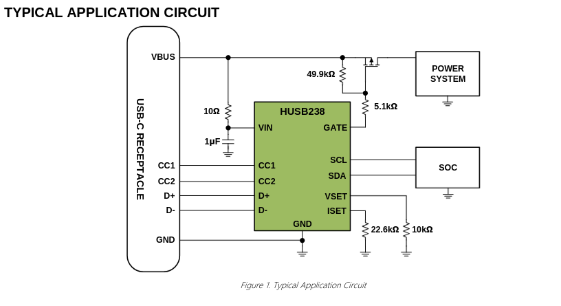
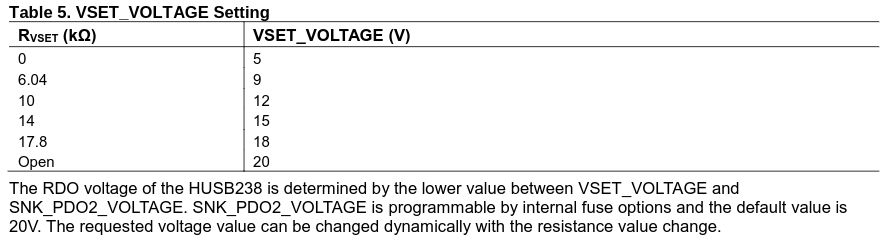
According to the VSET pin table in the datasheet, I need a 0k resistor (meaning just bridge it to GND) for 5V
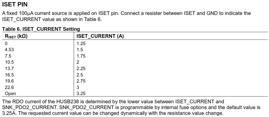
According to the ISET pin table in the datasheet, I need a 22.6k resistor for 3A of current
The Non display parts of the schematic
Okay, so lets start actually working on the schematic. I normally design in the following order
flowchart TB

power[Power] ---> microcontroller[Microcontroller]
microcontroller ---> specialstuff[Special Stuff]
I decided to switch voltage regulators to the SED5120, due to it being much easier to solder. And 1 and a bit hours in, I have a the basis of the power supply
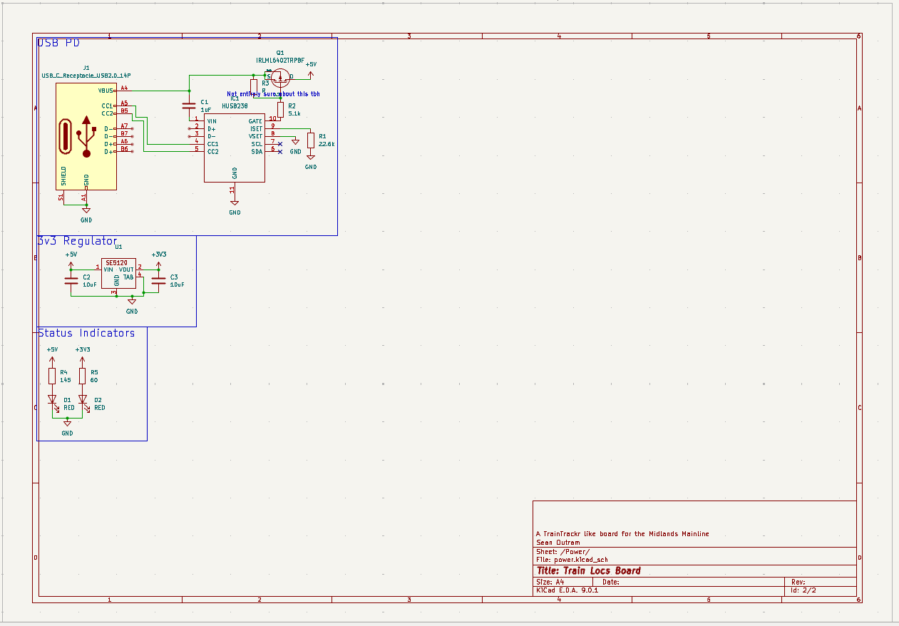
Now, time to start on the Microcontroller. I'm including 3 status LEDs on the board, this is because they are an easy way to see the state of things.
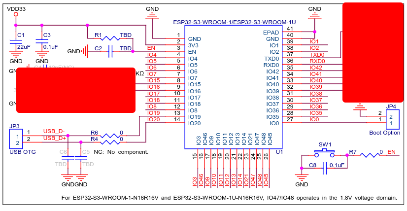
The ESP32 module reference schematic is this (when I remove everything which is actually not connected:
 It also occured to me that I needed a shift register, because driving neopixels from 3.3v is kinda cursed, especially with 105 of them. So I chose TI's TXB0106PW

The Display
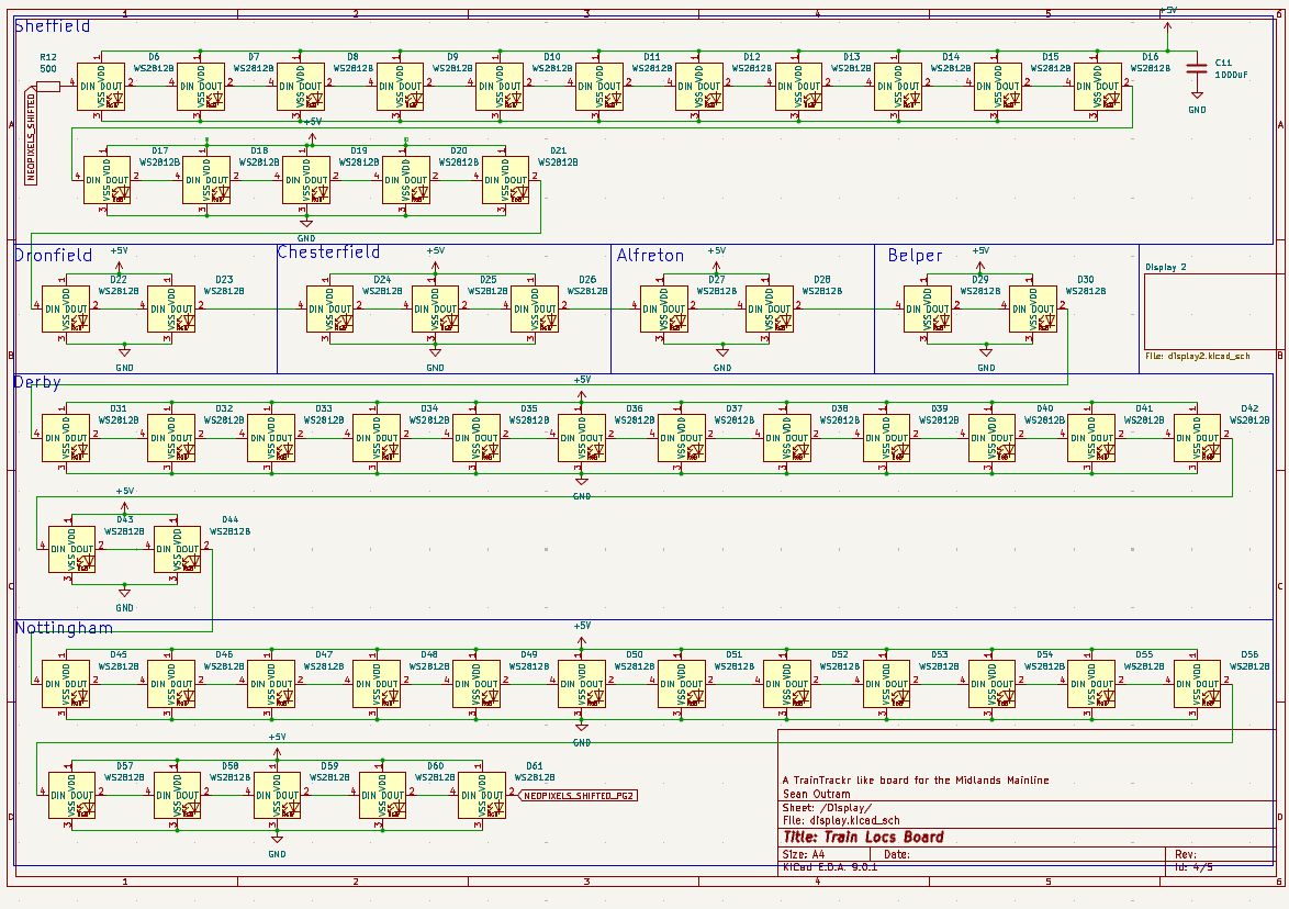
This is the whole 105 leds bit, I started by placing all the leds for each station linked together going from lowest -> highest platform number. I also decided to place a 1000uF capacitor at the start of the chain to help handle sudden current changes across the string.
I later decided to put one on each schematic page (of which the display elements became 2)
Actually doing the layout (The fun part :p)
At this point I needed to go track down footprints for it all.
Specifically: - The USB C - The button - The Mosfet
I went and used easyeda2kicad to download the footprints for the button, mosfet and voltage regulator.
Oh, and I was joking about the layout, I get to do more design.
The first step was to take the station layouts, and turn it into a figjam diagram.
And like an hour later with a bit of guesswork, I got this!
07/06/2025
I then needed to take the figma design, into an inkscape design (We will get to layout soon, I promise)
An hour ish later me, realised it would be a good idea to put the ESP32 on first, so that is what I did.
08/06/2025
I continued laying out the ESP32 today, I realised It would be a good idea to rotate it, and I shifted around the pins to make it easier to route.
I also realised I forgot the reset circuitry (whoops), so I added it roughly following the reference schematic.

And, like half an hour later, I have a fully completed ESP32
After my first 3 stations, I took this screenshot. I decided eventually to just place it all down in my PCB directly, without inkscape.
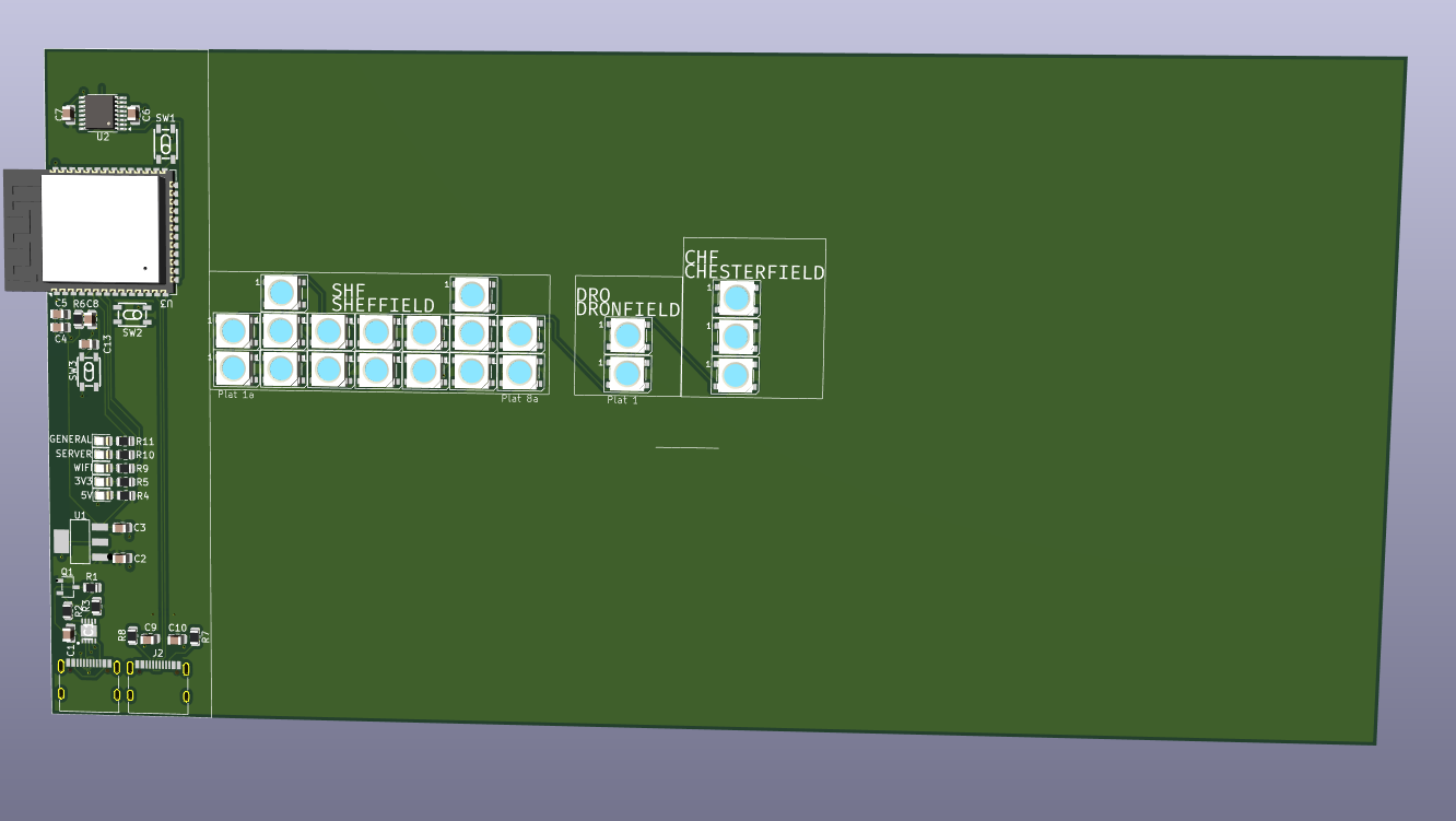
And a few more stations (and time) I got to this
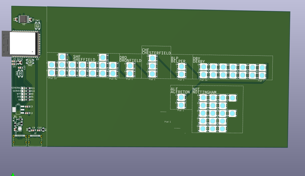 I also decided to move the
 stations
closer together.
At this point I considered deleting the additional boxes and station text, to bring it more inline with my reference artwork. but I am yet to come to a descision.
The above, I did indeed do. I also gradually found issues with my display schematic, where various things were not connected properly.
And, a little more time later i got this:
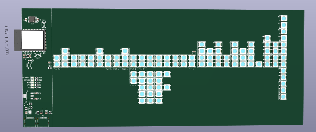
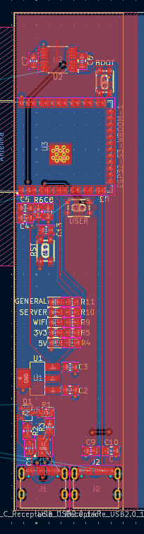
Now, I just need to clear up the silkscreen. Put mounting holes in and run DRC and stuff
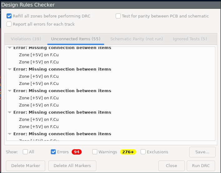
Oh, oops:
To make my life easier, I made the PCB 4 layers, where 1 inner one is a completely undisturbed 5v plane, This is to help with routing and handling the 3A of current.
15/06/2025
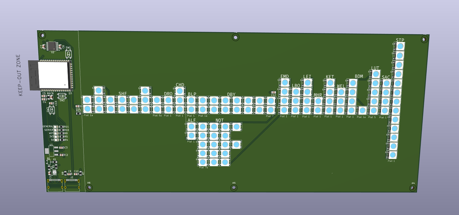
Today, I decided to (finally) place my mounting holes. I decided on 6 to allow for more stability when it is mounted to it's frame. The layout I went for is
X X X
X X X
I also continued working on the DRC errors. But as you can see, I have a while to go

A fair few of these were thermal relief spokes being 1 not 2, so I fixed that. Additionally, quite a few others were due to the spacing of the USB C connector. This is fine in reality and JLC will manufacture it anyway.
A few other DRC errors were related to the vias in the ESP32's GND pad. The size of these cannot be changed without modifying the footprint, However. 0.2000mm does fall above the minimum size requirements of JLC, so I adjusted my DRC settings to match.
And now, with a bit of work. I'm down to

I also realised at this point, I do need to somewhat label stations. I chose to do this via the Station Code.
And here it is!
A sensible person (not me) would go find the missing 3D models, although it's not getting a complete case, so the height of the components does not really affect me?