
Nixie Pendant
21/05/2025
Some basic goals:
- 2 Nixie Tubes
- Fully self contained
Safe
- Powered by a battery or USB
Choosing a tube
I went for IN-16 tubes, due to them being vertical. They are also relatively affordable on Ebay.
IN-16 digits use 2mA and run at 170v, The dot uses .3mA. These tubes have a diameter of 13mm.
A rough 2D Design
I then set out to design the rough 2d (top down) shape in Figma. This allowed me to plan out screw positioning and have a template for PCB shape.
This, while Rough Describes kinda what I'm thinking. The red circles are where the tubes are going, and the little whitish dots are where the 3 screws will go

I do need to remember that it is 4x actual size.
The plan is 3 long screws that will go the whole way through the body.
The Physical Stackup
Physically, it's going to be stacked up in a few different layers, In order of top to bottom: 1. Socket PCB (Tubes are soldered into here, will be sturdier than using an actual socket 2. High Voltage PCB (The control transistors, Boost Converter etc) 3. Low Voltage PCB (Battery Management, Charging, Micrcontroller 4. Battery
24/05/2025
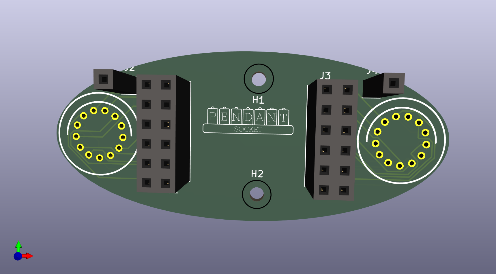
Today I started/continued designing the socket PCB. This is simple as it just holds the tubes in a way that can be disconnected.
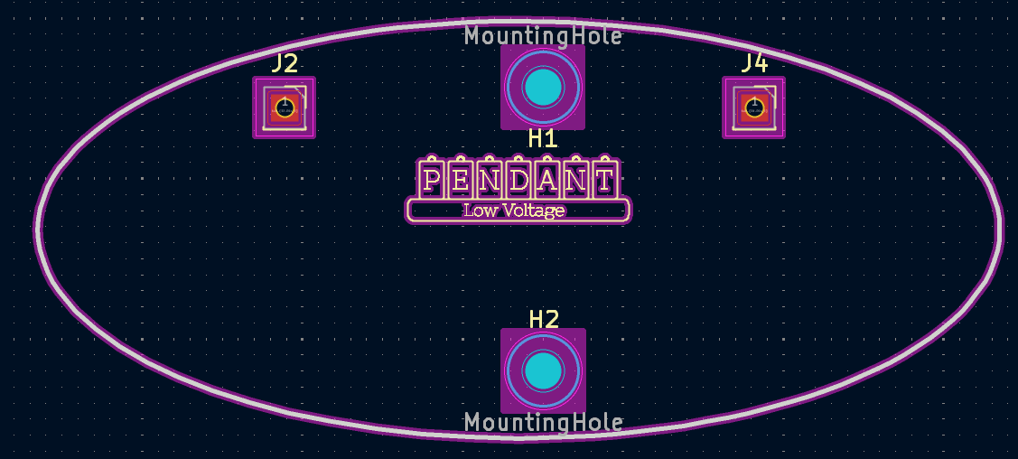
I need 3 different PCBS total, all with a consistent shape and like screw positioning, so I started designing a template.
I tried Figma but had issues with the PX to MM conversions, but I was able to get an oval layout in Inkscape.
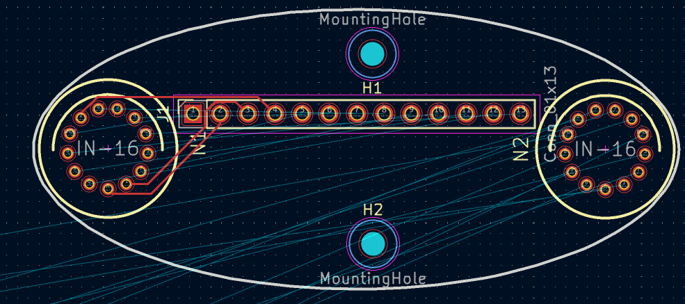
I originally tried this:
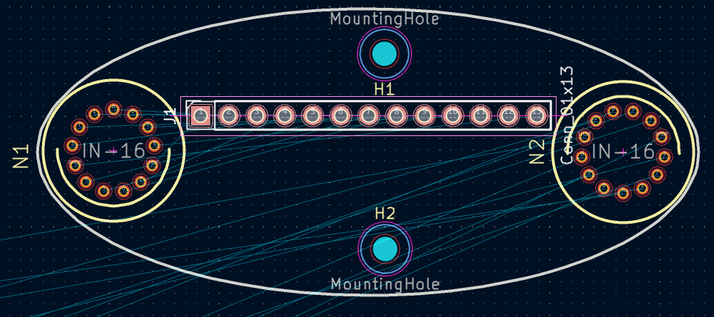
Unfortunately, my 1x13 pin header footprint did not fit.
So, I switched to a 2x6 and a 1x1 header for each tube. I also decided to just hard wire it to save space.
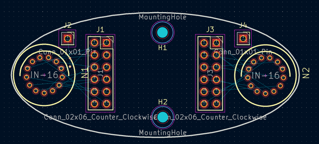 ,
I got it routed too :) (Yes the routing is horrible, but do better on a 2 layer PCB)
,
I got it routed too :) (Yes the routing is horrible, but do better on a 2 layer PCB)

25/05/2025
Today I started working on the Low Voltage Electronics (Battery Management/Charging and the RP2040).
The first step was copying across the board shape. To do this I just copied the sockets PCB file, and started removing stuff.
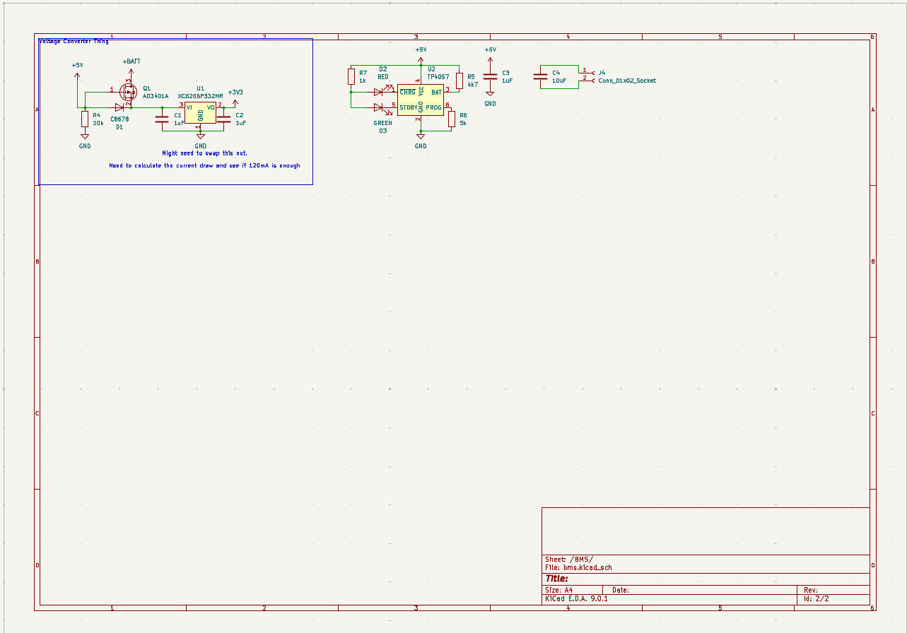
I started with the power circuitry, because that helps to layout the rest of the components. I think I may have to swapout the chosen LDO later, as I am unsure if 120mA will be enough current.
I debated using a battery protection IC, but I eventually concluded it wasn't worth the additional complexity. I also chose a battery capacity of 200mA, using a 5k resistor on the battery charger.
I then moved onto the RP2040 circuitry, I like making big and complex programs, so I went for the biggest flash I could :)
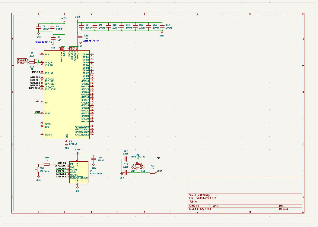 This does not have the IO for the High Voltage switching, as I am not sure what I want to use for it.